Application Hints
STV8172A
6/14
STMicroelectronics Confidential
4.1.1.1 Centering
Display will be centered (null mean current in yoke) when voltage on pin 7 is (R
1
is negligible):
4.1.1.2 Peak Current
Example: for V
m
= 2 V, V
M
= 5 V and I
P
= 1 A
Choose R
1
in the1
W
range, for instance R
1
=1
W
From equation of peak current:
Then choose R
2
or R
3
. For instance, if R
2
= 10 k
W
, then R
3
= 15 k
W
Finally, the bias voltage on pin 7 should be:
4.1.2
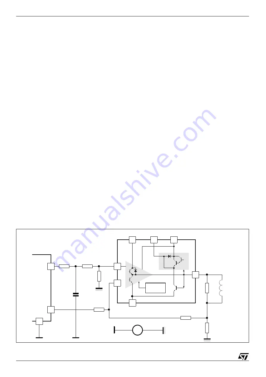
Ripple Rejection
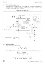
When both ramp signal and bias are provided by the same driver IC, you can gain natural rejection
of any ripple caused by a voltage drop in the ground (see
Figure 5
), if you manage to apply the
same fraction of ripple voltage to both booster inputs. For that purpose, arrange an intermediate
point in the bias resistor bridge, such that (R
8
/ R
7
) = (R
3
/ R
2
), and connect the bias filtering
capacitor between the intermediate point and the local driver ground. Of course, R
7
should be
connected to the booster reference point, which is the ground side of R
1
.
Figure 5: Ripple Rejection
V
7
V
M
V
m
+
2
------------------------
R
2
R
2
R
3
+
----------------------
è
ø
ç
÷
æ
ö
´
=
I
P
V
M
V
m
–
(
)
2
-----------------------------
R
2
R
1
xR
3
-------------------
´
=
R
2
R
3
-------
2
I
P
R
1
´
´
V
M
V
m
–
-----------------------------
2
3
---
=
=
V
7
V
M
V
m
+
2
------------------------
1
1
R
3
R
2
-------
+
-----------------
´
7
2
----
1
2.5
--------
´
1.4V
=
=
=
R
3
R
2
R
1
Rd
Yoke
Ly
Power
Amplifier
Flyback
Generator
Thermal
Safety
7
3
2
5
6
1
4
+
-
R
7
R
8
R
9
Reference
Voltage
Ramp
Signal
Driver
Ground
Source of Ripple


