background image

T

T

T

T

GND

GND

GND

GND

GND

GND

...

.............

DD-MM

DD-MM

DD-MM

DD-MM

...

...

...

...

...

...

...

...

...

4-14-2009_15:28

...........

...

...

...

...

...

...

DD-MM-YY

......

ADDRESS1

ADDRESS2

TELEPHONE

ADDRESS3

OF  :

PAGE:

ON:
BY:

BY:

ON:

CHECKED

DATE

Last saved :

DESCRIPTION

Last modif

NAME

A

3

2

1

F

E

D

C

B

8

7

6

5

5

4

3

2

1

THIS DRAWING CANNOT BE COMMUNICATED TO UNAUTHORIZED PERSONS COPIED UNLES S PERMITTED IN WRITING

F

E

D

C

B

A

4

6

7

8

FORMAT DIN A2

Index-Lab

DESIGNATION

SBU :

TCLNO:

DRAWN

TCL

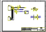
VGA_SCL

VGA_SDA

VSYNC

HSYNC

BP

SOG

GP

COM

RP

SOY1

Y1

COM1

PB1

PR1

SOY0

Y0

COM0

PB0

PR0

VDAC_OUT

CVBS1

CVBS0

ADCINP_DEMOD

ADCINN_DEMOD

AVDD33_RGB_STB

AVDD33_VIDEO_STB

AVDD12_DEMOD

AVSS33_CLN

CVBS_COM

AVSS33_RGB

AVSS33_VIDEO

IF_AGC

RF_AGC

DU2

VCC

DU1

S

DU3

DU4

W

DU5

VSS

DU6

DU8

DU7

Q

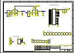
HOLD

C

D

AIN_L0

AIN_L1

AIN_L2

AIN_L3

AIN_R0

AIN_R1

AIN_R2

AIN_R3

AL0_ADAC

AR0_ADAC

AL1_ADAC

AR1_ADAC

ASPDIFI

ASPDIFO

AOMCLK
AOBCK
AOLRCK
AOSDATA0
AOSDATA1

VMID_AADC

AVDD33_ADAC
AVDD33_AADC

AVDD33_CAP

DIO

CLK

HOLD

VCC

GND

WP

DO

CS

SDA

SCL

WC

VCC

VSS

E2/NC

E1/NC

E0/NC

GND

T

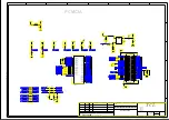
IIC ADDRESS "A0"

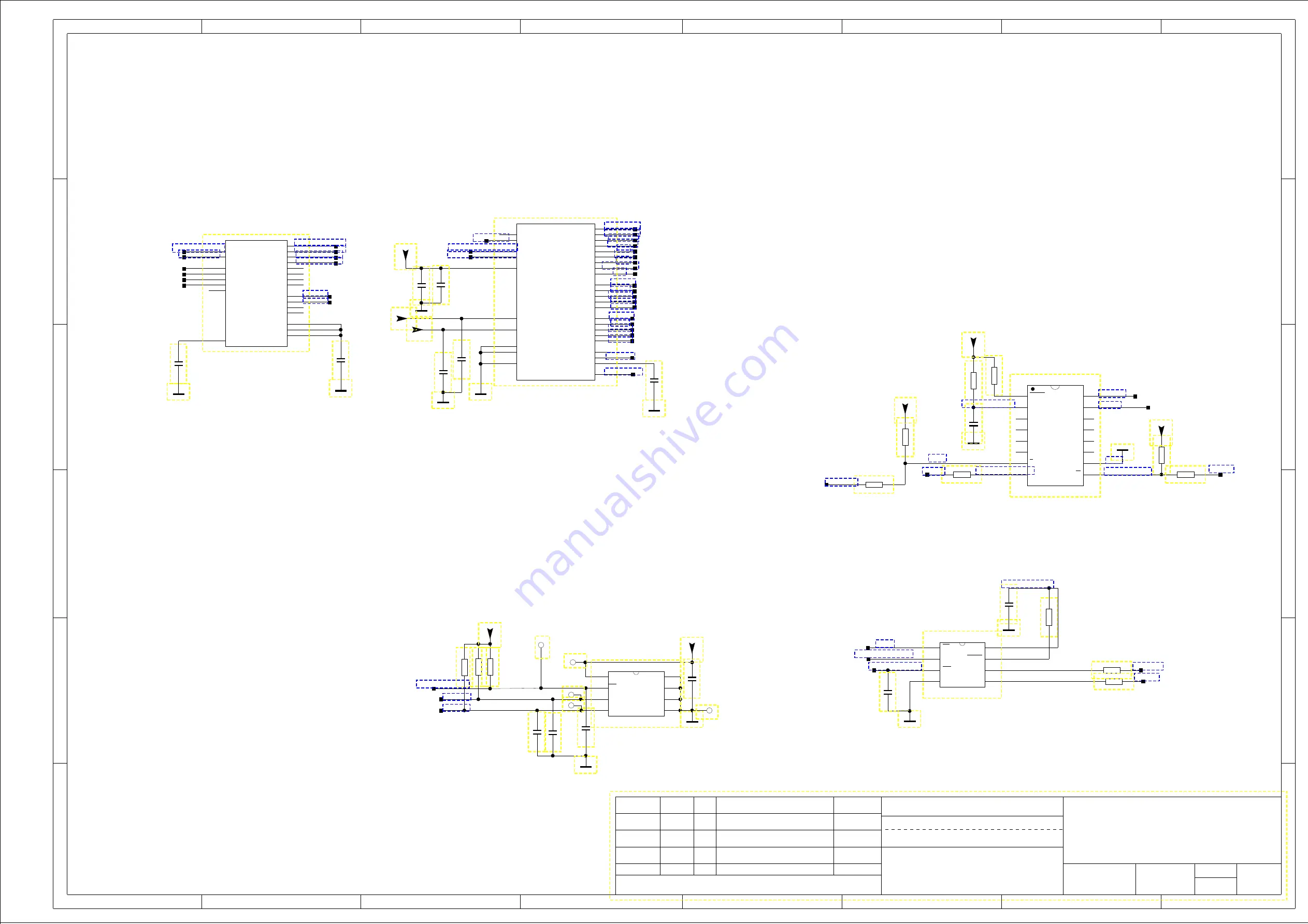
Serial Flash

Audio&Video

VCC_FLASH

PDD6_FLASH

FLASH_WP#

PDD6

CS#

PDD7

POOE#

R703

0R

PDD6_FLASH

AVDD3V3

AVDD3V3

OSDA0

EP-VCC

R716

4K7

2K7

R715

R714

2K7

VMID_AADC

3V3SB

3V3SB

C704

1U

C702

0.1U

C701

0.1U

AVDD1V2

5

6

7

8

4

3

2

1

U703

M24C32MN

SYS_EP_WP

C714

0.1U

C713
0.1U

5P6

C712

C711

5P6

C710

0.1U

FLASH_WP#

C706

0.1U

5

6

7

8

4

3

2

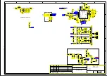
1

U702

W25Q64FV

CS#

SCART1_L_IN

SCART1_R_IN

VDAC_OUT

CVBS_COM

CVBS1P

PR0P

PB0P

COM0

Y0P

SOY0

PR1P

PB1P

GP

SOG

BP

RP

VGACOM

HSYNC

VSYNC

VGASDA

VGASCL

ARC_OUT

SPDIF_OUT

U20

V20

T20

T19

R20

R17

R19

R18

R16

P16

T18

U19

F16

R4

R2
R1

P3

R3

T4

T16

M16
M14
L15

U401

MT5531

4

2

3

7

5

6

9

11

10

12

14

13

8

1

16

15

U700

NC/M25P128

NC/4K7

R713

V5
V4
V10
U10
V11
U11
W12
Y12
V12

U12
V13
U13
W14
Y14

V14
U14
V15
U15
W16

W17

Y17

V18

W18

Y19

V17

U17

Y20

N14

Y16

T12

T14

J15

L16

U401

MT5531

R709

4K7

R708

0R

C705

1U

C709

0.1U

C703

0.1U

C700

1U

R702

NC/0R

R701

4K7

0R

R700

C707

0.1U

DVDD3V3

DVDD3V3

DVDD3V3

AR0O

SDATA0

ADCINP_DEMOD

IF_AGC

LRCK

BCK

MCLK

AL0O

YPBPR_L_IN

YPBPR_R_IN

PDD5

VCC_FLASH

POCE0#

GND

COM1

Y1P

SOY1

ADCINN_DEMOD

R712

10K

R711

0R

0R

R710

PDD7

POOE#

Z701

EP-WP

EP-SDA

EP-SCL

OSCL0

Summary of Contents for 32T3510

Page 1: ...ent Procedure 7 4 Block diagram 1 5 Scheme Diagram 5 Troubleshooting 2 6 PCB Layout 3 SORGH GUDZLQJ This m anual i s t he l atest at t he t ime of pr inting and doe s not include the modification whic...

Page 2: ...ectric shock to the person The exclamation point within an equilateral triangle is intended to alert the user to the presence of important operating and maintenance servicing instructions in the liter...

Page 3: ...impact of any kind Be particularly careful not to damage the picture tube surface 9 Unplug this television set from the wall outlet before cleaning Do not use liquid cleaners or aerosol cleaners Use...

Page 4: ...ng conductors location of antenna discharge unit connection to grounding electrode and requirements for the grounding electrode 15 2 Note to CATV system installer Only for the television set with CATV...

Page 5: ...durein youroperatinginstructions do not attempt any further adjustment Unplug the set and call your dealer or service technician 22 Whenever the television set is damaged or fails or a distinct change...

Page 6: ...MT5531 EU AU RU Series Version 0 90 MT31L Low Cost CCFL LED Platform MT31D Low Cost CCFL LED Platform for E3000 ID only MT31B Basic Entry Level LED Platform MT31BT LT DT DVB T2 Chassis LED Platform M...
Page 7: ...x and 0 012 for y Add Project White Balance Information v0 40 2013 04 12 Add MAC upgrade method by USB Upgrade MTK Tool for MT31 v0 50 2013 04 18 Mr Christian upgrade information Add PQ engineer Note...

Page 8: ...TV DVB T C DVB T C DVB T C DVB T C DVB T C MPEG 2 MPEG 4 DVB T2 DVB S2 DVB T2 HDMI CEC MT31B D 2 MT31L 1 MT31B D 2 MT31L 1 MT31B D 2 MT31L 1 MT31B D 2 MT31L 1 2 480i p 576i p 720p up to 1080i p compli...

Page 9: ...N A N A Audio Return Channel Others Serial connector N A N A N A N A N A VGA connector P1000 P1000 P1000 P1000 P1000 I2C connector of MEMC module N A N A N A N A N A Class Item MT31B MT31L MT31D IC D...

Page 10: ...following snapshot further details are described on below sections INFO All tests and measurements mentioned hereafter have to be carried out at a normal mains voltage 220 240 VAC All voltages have to...

Page 11: ...e Appendix How to upgrade FLASH SW using MTK tool See Appendix How to upgrade FLASH SW using USB OAD Transport Stream Image To manage quicker mass reflashing a predefined OAD DVB T channel freq 850MHz...

Page 12: ...facing up TV see below Product Assembly section 2 0 how to activate Factory key The SoC s RS232 mode is automatically enabled at power on and doesn t require any command initialization frame 0x30 0x30...

Page 13: ...Test Once the boards chassis KB IR PSU and the panel are well interconnected plug all suitable signals generator to relevant below inputs outputs using respective test patterns format to check pictur...

Page 14: ...Audio Control Audio Return Channel RJ 45 IP Return N A Headphone RF signal N A Loud Speakers Enclosures RF signal Suitable channel Picture Video formats and Audio tones can be changed by the factory a...

Page 15: ...ent 2 1 Factory Menu Follow the below steps to pop up the Factory menu in case of FactoryKey is disabled Press RCU MENU key to display main menu Select Picture and press OK key to enter into Picture s...

Page 16: ...3 Warm up Test Following TCL standard and practices it s required minimum 15min of Warm Up that can be considered as Burn In Additional Aging for White Balance alignment is no more necessary due to co...

Page 17: ...lue The measured and adjustable parameters should be mainly x y coordinates see TCL EU Picture Quality Requirements for FPDs for reference The signal level check has been down in R D Factory should no...

Page 18: ...16 0 27 A L32F3303 H3 32F33Q9 WE1AWAA 270 280 280 290 315 327 3 0 9 128 128 131 16 0 27 A L32F3393 H3 32F33Q9 WE1BWAA 270 280 280 290 315 327 3 0 9 128 128 131 16 0 27 A L32HW3323 H3 32E33S3 WE1DWAA 2...

Page 19: ...8 128 128 16 0 27 A 32HU3253C H3 32E33S3 WE1PWAA 270 290 280 302 317 341 3 0 9 128 128 128 16 0 27 A L32E3003 H3 32E33S3 WE1NWAA 270 290 280 302 317 341 3 0 9 128 128 128 16 0 27 A L32E3005 H3 32E30X1...

Page 20: ...v5 9 2 4 High Pot and Insulating Resistance Tests At the end of the process a High Voltage and an Insulating Resistance tests are required to fulfil Safety Electrical requirements CEI 65065 High Volt...

Page 21: ...anufacturing TV input connector note that PC connector requires TVs on Factory mode Launch MTK tool with version above v0 6 7 Set right SoC template ex MT53xx Select Tool button Press Browse button to...

Page 22: ...dow script When upgrade is completed remove UART connection Restart SSB chassis or TV and wait few seconds for Eeprom update Remember to perform Factory menu Reset ALL and then press RCU OK key if the...

Page 23: ...Factory mode caption info or on bottom of Factory menu B Upgrade without Loader Customer mode Copy the corresponding SW PKG image ex V8 0MT310x LF1Vxxx pkg into USB stick pen drive root path and rena...

Page 24: ...lashing will be skipped acknowledged by default Once upgrading completed TV may restart automatically after warm start and implicit ResetAll in case of NVM mapping signature change in previous Factory...

Page 25: ...the computer ESC key when hold on TV waiting for TV finish up after the upgrade Appendix How to upgrade CI Key using USB Copy corresponding key files into USB stick pen drive root path and renamed the...

Page 26: ...iles filter then browse any key file like below snapshot Modify Custom Burning Address to 790000 then start to upgrade Restart TV Go to Factory menu Other Update CI Credential Update CI Credential the...

Page 27: ...B CMP Select by pressing key Color Temperature Normal Warm Cool Select Tone by pressing key RED Gain 000 255 Set R Gain by pressing key 127 128 for offset GREEN Gain 000 255 Set G Gain by pressing key...

Page 28: ...gh by pressing key 127 128 for offset Scaling Contrast 000 255 Set ScCont by pressing key 127 128 for offset Scaling Saturation 000 255 Set ScSat by pressing key 127 128 for offset Lightsensor Setting...

Page 29: ...Channel Map Pre Frequency Thailand Press OK key to preload TH Channel Map 8 Power Mode submenu Item Sub item Value Note Power Mode Always On Standby Last Status Select starting sequence by pressing ke...

Page 30: ...MT25F0x LF1Vxxx Date Info Time Info MTK Version Info ex _002204_4_001_1_002 RCU Info PSU Info Region Info Product S N Info Update MAC address Update from USB Press OK key to copy MAC address from USB...

Page 31: ...ignment Specification for MT5331 Series v0 91 Page 26 of 26 Note A quick access to suitable submenu item can be achieved by pressing it prefixed RCU key number ex pressing 9 to directly highlight USB...

Page 32: ..._2 RX_0_2B HDMI_CEC HDMI_0_HPD HDMI_CEC MHL RX 0 C RX 0 CB RX 0 0 RX 0 0B HDMI 0 SDA RX 0 1 RX 0 1B HDMI 0 SCL RX 0 2 RX 0 2B DVB T2 DEMO PCMCIA SCT1_AV_OUT U0RX U0TX CI_MIVAL CI_MCLKI CI_MCLKO CI_RES...

Page 33: ...1U C161 10U C160 10U R101 NC 6R8 C155 NC 470P NC 390P C139 C145 3300P 10N C140 470P C154 R168 0R DIM_IN C100 220U 16V C157 10U NC 10R R118 DIM_IN 1 2 3 6 5 8 4 7 U104 RT8110D 3D_CTRL 3D_SEL KEY_PAD 1...

Page 34: ...ngapore Pte Ltd 8 Jurong Hall Road 28 01 06 Tel 65 63092900 Fax 65 63092999 TCLNO DESIGNATION XOUT IF_N IF_P ANT SCL 3V3 SDA GND IF_AGC 300mA Close to MT5531 Close to MT5531 6 7 8 1 3 2 4 5 9 TUN2 6 7...

Page 35: ...R344 75R R346 75R C332 33P 1 2 P301 F320 R337 220R SPDIF_OUT C326 0 1U R307 120R R322 100R R320 100R C310 1500P R341 0R R342 75R R343 0R R345 0R 47P C307 R315 75R 0R R302 R305 33K 2U2 C301 R314 10K R...

Page 36: ...dex Lab DESIGNATION SBU TCLNO DRAWN TCL GND CLOSE TO MT5531 CLOSE TO MT5531 SCART1 Audio Output core power close to chip DDR IO POWER close to chip POWER INTERFACE DDR3 POWER close to Main chip Close...

Page 37: ...I_VCC CI_VCC R526 10K CI_DVDD3V3 CI_DVDD3V3 C502 0 1U R525 10K 5V CI_VCC C504 0 1U CI_DVDD3V3 AVDD3V3 R524 47R R523 47R R522 47R R521 47R R520 47R R519 47R R518 47R R517 47R R516 47R R515 47R R514 47R...

Page 38: ...CFG_PWM1 R639 NC 100R 3D_VSYNC_IN PWM0 3D_VDD MEMC_POWER 12V R608 NC 1K R613 4K7 R611 33K G D S Q601 PMV65XP R632 NC 0R R631 NC 0R R630 NC 0R C611 27P C608 27P X600 24M C607 10P NC R601 NC 0R R607 0R...

Page 39: ...1 NC E0 NC GND T IIC ADDRESS A0 Serial Flash Audio Video VCC_FLASH PDD6_FLASH FLASH_WP PDD6 CS PDD7 POOE R703 0R PDD6_FLASH AVDD3V3 AVDD3V3 OSDA0 EP VCC R716 4K7 2K7 R715 R714 2K7 VMID_AADC 3V3SB 3V3S...

Page 40: ...J20 J19 K16 J17 J14 K15 J16 J18 K14 L17 H20 U401 MT5531 AVDD1V2 C804 0 1U AVDD1V2 HDMI_CEC R806 100R HDMI 0 SCL HDMI_0_SDA HDMI_0_SCL RX_0_2 2 1 4 3 EXC24C L802 2 1 4 3 EXC24C L801 2 1 4 3 EXC24C L800...

Page 41: ...6R8 R902 6R8 AMP_RESET R950 0R L900 R 35V NC 220U C908 C903 1U C906 1U 47 46 45 44 43 42 41 40 39 38 37 35 34 33 32 31 30 29 28 27 26 25 24 23 22 21 20 19 18 17 16 15 14 13 11 10 9 8 7 6 5 4 3 2 1 36...

Page 42: ...04 SOG C1007 0 01U C1009 NC 10P C1008 NC 10P RP VGACOM GP BP C1002 NC 10P C1001 NC 10P C1000 NC 10P R1004 10R R1005 100R R1001 75R R1000 75R VGA TXD C1004 0 01U C1005 0 01U VGA5V HSYNC VSYNC B G R VGA...

Page 43: ...4 15 16 17 18 19 20 21 22 23 24 U1101 CXD2837ER C1151 NC 0 1U L1104 NC 220R L1100 200R T2_1V1 C1118 NC 10P 1 2 3 4 5 6 7 8 R1126 10R T2_1V1 0 1U C1138 C1107 0 1U 5V C1106 1U 10P C1130 R1114 100R 3V3_D...

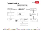
Page 44: ...ower board Check every DC DC module Check if main chip Output Pow ON Dim BL ON Signal to power board Check the U401 main IC Peripheral components upgrade main software check whether it connect ground...

Page 45: ...icture in all source Check the relevant signal source circuit Check peripheral components of U401 U401 Problem Check the circuit between U401 to panel Check the LVDS connector and T con board and pane...

Page 46: ...l sound Abnormal sound in all source Check the relevant signal source circuit Check the waveform of P902 OK Check the status of IIS OK Check Speakers Y Check the status of U900 AMP_VC C mute reset OK...

Reviews: