background image

新建文件夹

  (3)Test  and  Alignment  Specification  for  NT63 

Series    (v0  01)  170612


Page 12 of 25 

2.3. White Balance   


White Balance Touch-Up (Golden sample) 


As some color coordinates discrepancies can be noticed from panel batches to others, it may necessary to perform 

slight touch-up.   

For Color temperature adjustment, switch TV on leading 

HDMI 

input where should be connected suitable generator 

providing following format 

1280x720p@60Hz

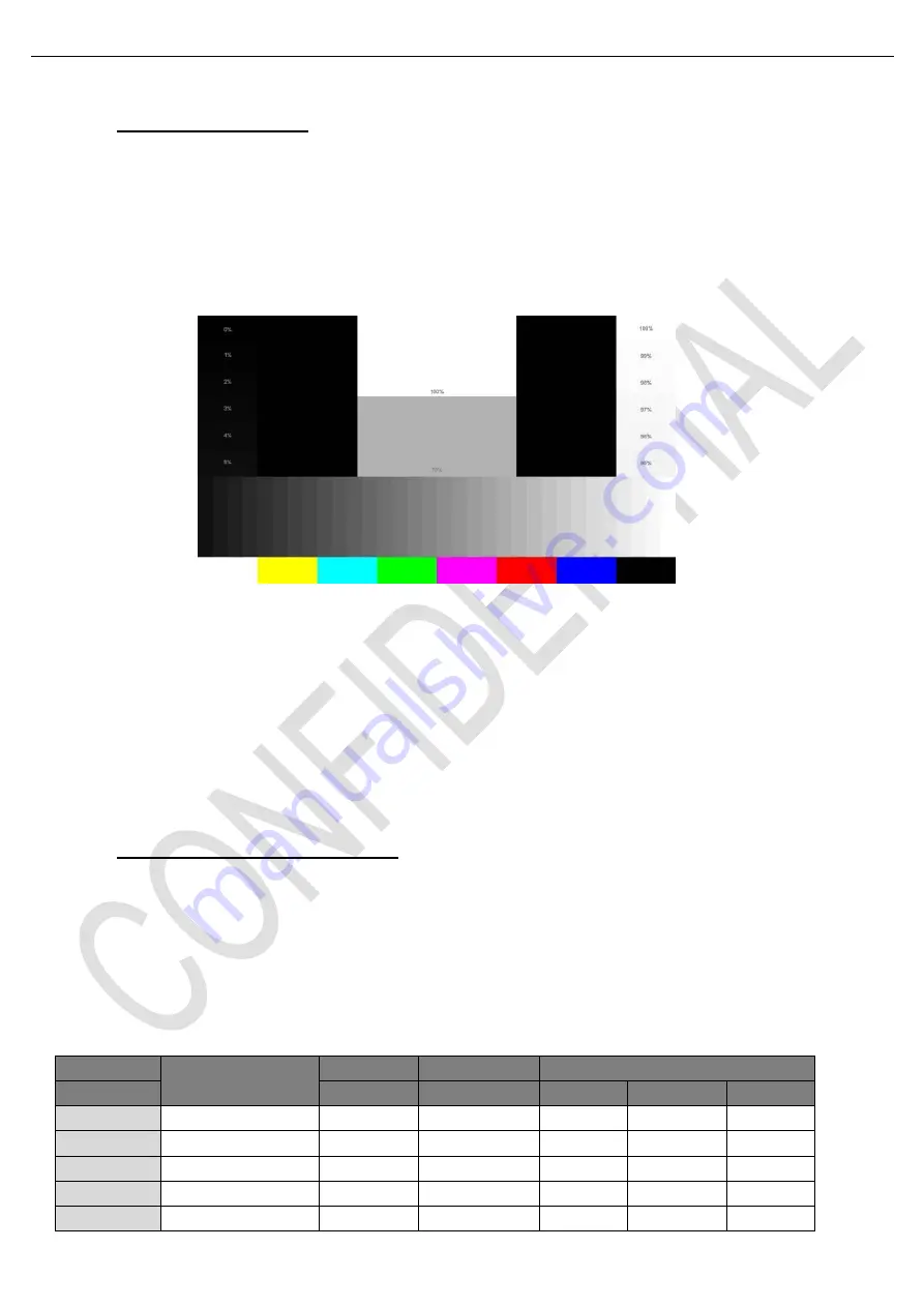
 test pattern. A 32 steps grey scale is recommended to assess relevant 

colorimetry tracking and low/high light saturation points. 


Ensure that TV’s picture enhance is off.


Ensure  that  TV  is  in 

Factory  mode  to  access  to  ”

White  Balance

”  adjustment  submenu

,  then  scroll  down  to 

toggle off “

Pic. Enhance

” flag.   

WB Normal is the first mode which is adjusted in HDMI source

the next are HDMI warm and cool mode. 

Warm

 and 

Cool

 Tone are relatives to 

Normal

 mode.


WB adjust need to fix default G Gain .Offset registers needn

’t 

to be adjusted. 


Gain

” registers set need to be adjusted at 70IRE.


Targets and Tolerances for all inputs 

  (According to company uniform LED color temperature standard of panel)   


The measured and adjustable parameters should 

be mainly “

x

”, “

y

” coordinates. 

The White Balance alignment should be performed using a well calibrated and contact less analyzer (ex: Minolta 

CA210 or CA310). The analyzer may not touch the screen surface, and measurement must be performed in a dark 

environment keeping the probe(s) at 90+/-2° from the panel center. 

The results should fulfill specification for each 

TV set

 offered by R&D and below tolerances:: 


NT72563 

panel name 

Energy 

FW Min (Nits)  Preset Targets (x, y) 

Model 

Efficient 

FW>Min 

COOL 

NORMAL 

WARM 

43D2900 

ST3151A05-9 

A+ 

250 


Summary of Contents for 39S62

Page 1: ...n 3 Alignment Procedure 4 Block diagram 5 Scheme Diagram 6 Troubleshooting SORGH GUDZLQJ This m anual i s t he l atest at t he t ime of pr inting and doe s not include the modification which may be ma...

Page 2: ...ectric shock to the person The exclamation point within an equilateral triangle is intended to alert the user to the presence of important operating and maintenance servicing instructions in the liter...

Page 3: ...impact of any kind Be particularly careful not to damage the picture tube surface 9 Unplug this television set from the wall outlet before cleaning Do not use liquid cleaners or aerosol cleaners Use...

Page 4: ...ng conductors location of antenna discharge unit connection to grounding electrode and requirements for the grounding electrode 15 2 Note to CATV system installer Only for the television set with CATV...

Page 5: ...durein youroperatinginstructions do not attempt any further adjustment Unplug the set and call your dealer or service technician 22 Whenever the television set is damaged or fails or a distinct change...

Page 6: ...l Flashing Off Basic Function Yes for user setting in TV first starting a special standby mode for starting less than 4s Ethernet Network In Center of Front white in Standby YouTube NETFLIX WiFi integ...

Page 7: ...ent from smartphone to TV Connect Mobile phone to TV sets and control the TV like Remote Control T CAST Mechanical ID Picture W1 mm 887 Carton Dimensions WxDxH mm 1049 144 638 D1 mm 83 Container Loadi...

Page 8: ...gnment Specification for NT63 Series v0 01 170612 Page 1 of 25 TCL World Wide R D FPD CENTER Test Alignment Specification TAS for NT72563 Version 1 0 PREPARED BY DATE 2017 6 12 CHECKED BY DATE APPROVE...

Page 9: ...ormation contained in this document is proprietary to TCL SZ FPD lab and shall not be disclosed by the recipient to third persons without the written permission of the team leader or GM of R D Revisio...

Page 10: ...ification for NT63 Series v0 01 170612 Page 3 of 25 These chassis are designed for European LCD TV markets Ready for IPTV The main chip is from novatek NT72563 series with embedded Linux core and supp...

Page 11: ...N563T01 LF1VXXX UF1 4GB V8 N563T01 LF1VXXX HDMI SWITCH EDID BIN image N A N A Manufacturing Connectors Pinout ISP UART P15 Pin1 NC Pin2 RXD Pin3 TXD Pin4 GND USB to UART Bridge Adapter FT2232D chipset...

Page 12: ...3 Test and Alignment Specification for NT63 Series v0 01 170612 Page 5 of 25...

Page 13: ...iagram and make sure that no serious issue or mistake can destroy the board For example the output of DC DC and LDO should not be shorted to ground Supply a suited voltage and power on then check the...

Page 14: ...to suitable UART device or an IR emitter device correctly facing up TV see below Product Assembly section 2 0 how to activate Factory key The UART parser engine is enabled by sending following command...

Page 15: ...080 1 Frequency Range full band 2 Standard PAL SECAM 3 DVB T C Satellite Tuner DiSEqC v1 0 A B C D and Tone Burst A B Double LNB frequency band change by 22KHz Tone Compliant DVB S S2 source from gene...

Page 16: ...according to VESA Enhanced EDID 1 3 and EIA CEA 861B for HDMI CEA Timing Extension structure has been extended to support all 3D capable timings All HDMI structures have their own BIN profile which ar...

Page 17: ...factory workstation LAN system Then during production lot it s necessary to send write all those codes to each TV DID codes can only be set using UART commands described above on enclosed SIACP requir...

Page 18: ...is enabled there s some toggled display information 2s relative to SW Project ID CI Network ID to facilitate 100 quick screening without accessing to whatever else menu Main SW Ver Project ID ID ERG P...

Page 19: ...first mode which is adjusted in HDMI source the next are HDMI warm and cool mode Warm and Cool Tone are relatives to Normal mode WB adjust need to fix default G Gain Offset registers needn t to be ad...

Page 20: ...images will be created overwritten or read on USB stick pen drive depending on chosen template like following database database db These files need to be used strictly with MT5655 SoC platform as depe...

Page 21: ...bin blank upgrade main software upgrade_loader pkg from the software website Connect UART interface to suitable manufacturing TV input connector upgrade boot bin first to blank IC 1 copy all files und...

Page 22: ...ge V8 N563T01 LF1Vxxx bin into USB stick pen drive root path Name V8 N563T01 LF1Vxxx bin as update zip please delete other xxx pkg files from USB stick Make sure the USB remaining available storage is...

Page 23: ...tID ex 001 If it works the TV will restart automatically Appendix 5 How to upgrade CI Key using USB Create a new folder named CI KEY on USB stick pen driver root path Copy corresponding key files into...

Page 24: ...bin HDCP2 bin into USB stick pen drive root path please pay attention to the spell Picture contrast 1950 Main Menu Go to Main Menu Service Menu USB UPDATE HDCP Upgrade HDCP2 0 Upgrade Appendix 8 How...

Page 25: ...ur wireless network you need a wireless router or modem and a Wireless LAN Adapter Connect your Wireless USB Adapter USB dongle delivered with your TV to your TV s USB Select Option Settings Network I...

Page 26: ...ress type to Manual by pressing OK key then press key to go to the first entry field Enter the IP address Subnet mask Default gateway Primary DNS and Secondary DNS values Use remote control digital ke...

Page 27: ...ect Download software will be download automatically The download progress will be shown in the lower right corner note Please follow the instructions on TV if download or update failed And you can ch...

Page 28: ...t Update TV will update automatically First the following dialog will be shown Then TV will restart automatically to finish updating note Please do NOT power off TV until it restart successfully You c...

Page 29: ...utomatically All the following operation is same as Update through the menu Appendix 11 Factory Menu Description 1 Factory Hotkey submenu Item Sub item Value Note Hotkey Off On Enable Hotkey flag by p...

Page 30: ...Set B Gain by pressing key 128 127 for offset R Offset 000 255 Set R Offset by pressing key 128 127 for offset G Offset 000 255 Set G Offset by pressing key 128 127 for offset B Offset 000 255 Set B...

Page 31: ...l Grey Ctrl Select Grey Ctrl ON or OFF by pressing key to control picture menu Grey or not Update CI Credential Update CI Credential Press OK key to remove CI key Update from USB Press OK key to copy...

Page 32: ...Update Main Upgrade Press OK to update Main software FRC Upgrade Press OK to update FRC software FRC Backup Press OK to copy FRC software to USB All Clone USB TO TV ALL UserData CH list Press OK to co...

Page 33: ...6 Power Supply Block Diagram 12...

Page 34: ...5 Chassis Block Diagram 11...

Page 35: ...5 AS1117 2 5 POWER_ON CD9 10U 0 1U CD10 12V 1 PW ON 220R RDJ5 RDJ1 100K NC RDC1 47K 10K RDC2 0 01U CDC4 1 2 NC ESD5451R D101 B C E Q02B BT3904 B E C BT3906 Q100 C126 470U 16V 0 01U C102 R103 10K NC 0...

Page 36: ...1 4 5 P204 C278 47P J16 L19 L18 K18 M23 L22 K22 M21 L21 K21 K20 J21 J22 J23 H22 K23 M22 J18 K19 H21 US1 NT72563 C21 B23 C22 A23 B22 D23 E21 E22 D21 D22 F22 F23 C23 G22 G21 G23 F21 U9 V9 W9 Y9 T10 U10...

Page 37: ...TU SDA1 CT35 22P CT36 22P CT34 22P CT33 22P LT11 1000R CT22 8 2NH RT51 0R RT50 0R CT13 1U TU_3V3 TU_3V3 19 11 16 17 8 7 6 5 4 3 2 1 13 24 14 23 22 21 20 18 15 9 10 12 UT1 MXL661 CT7 0 1U TU_3V3 RT53 1...

Page 38: ...11 4U7 I2S_LRCK I2S_DATA MAIN3V3 L 13 14 15 16 1 2 3 4 5 6 7 8 17 18 19 20 21 23 24 22 9 10 11 12 UA01 AD82587D AMP_SDA NC 15P CA07 CA05 15P NC NC 15P CA08 AMP_SDA MAIN3V3 RA99 4K7 RA98 4K7 AMP_SCL RA...

Page 39: ...C14 AC21 AA14 AC13 AB13 AA13 AB12 AB11 AC11 AA11 AC20 V16 Y18 V17 Y17 W17 Y14 W16 Y16 AC17 AB17 AA18 AB18 AA19 AB19 AC19 AA20 AB20 W18 Y19 US1 NT72563 D511 1N4148WS 15 16 2 5 8 11 17 19 13 14 7 9 4 6...

Page 40: ..._SEL GND GND NC PANEL_VCC SDA SCL WP LVDS_SEL Max3A LVDS Out FHD HD 60Hz FHD LVDS Test Point HD 14 2 3 4 5 6 7 8 9 10 11 12 13 15 16 17 18 19 20 21 22 23 24 25 26 27 28 29 1 30 P802 NC 12V_PANEL B10 C...

Page 41: ...1 2 9 10 11 12 PN1 16 15 14 13 12 11 10 9 8 7 6 5 4 3 2 1 TS8121CLF UN2 9 1 3 5 10 4 6 7 8 2 ESD UN1 CN6 10P NC CN5 1000P CN2 0 01U 0 1U CN1 RXC TXC 75R RN8 RN7 75R 75R RN6 RN5 75R CN3 1000P 2R2 RN4 R...

Page 42: ...AM_S_CKE DDRS_CKE_F DRAM_S_CKE DRAM_S_CKE DDRS_CLK GND R60 10K R58 12K R56 0R NC MMU_RSTN DRAM_S_RSTN DRAM_S_RSTN DDRS_CS0 R52 240R MAIN1V5 1K R418 R420 1K GND R50 240R C320 1000P C321 0 1U B3 R9 N1 N...

Page 43: ...RESET GND GND GND GND GNDGND BBS9 BBS13 close to eMMC close to eMMC BBS3 BBS19 BS9 1 w Security Boot BS9 0 w o Security Boot RESET need 50ms eMMC EMMC1V8 Boot Starp Note Please Check Application Note...

Page 44: ...PTSIN2_START DEMODOUT_START DEMOD_EMERGENCY GPC_4 ARM_UART_B_TX INT_5 ARM_UART_A_TX GPC_5 ARM_UART_B_RX INT_6 ARM_UART_A_RX GPC_12 INT_7_BS0_ GPC_13 INT_8 GPC_14 INT_9 USB1_D USB1_D GPD_24 CI_RST TC_P...

Page 45: ...J17 R15 J19 R17 M18 K14 D5 C5 C4 B5 B4 A5 P11 F1 P14 J14 N17 A1 J8 J9 J10 K6 M10 N2 N7 N8 N9 N10 M12 P7 P9 R1 R7 V2 AC1 AC23 G3 G4 K15 L2 AA3 AA4 A4 L15 K13 J13 P10 H19 M9 Y20 Y3 P15 M16 J20 N18 F2 N...

Page 46: ...TIVE GPB_23 CI_HAD6 I2S_OUT_C_WS LR0_DELAY GPB_24 CI_HAD7 I2S_OUT_C_DATA LR1_DELAY GPA_26 CI_CE BT_SHOP_VS_IN BT_SHOP_LR_IN GPB_6 CI_HA4 FRC_DIMMING1 DSU_BRE LEONDSU_BRE OPROC_DSU_BRE NAND_D4 GPB_7 CI...

Page 47: ...t Check software and ID number Replace main board Check CS01 and X12M Upgrade soft and select right ID Check Q601 Q600 working condiction Check UDF1 UDJ1 UDC1 output Check keypoints 5V Check UD1 outpu...

Page 48: ...s ok Check the audio amplifier power is 12V Check the audio amplifier power voltage is 3v3 Replace CA22 CA23 CA24 CA25 CA26 CA27 confirm Check UA01 output pin to LA02 LA03 LA04 LA05 Replace UA01 Check...

Page 49: ...onnector is ok Check software version and project id number Replace the main board to confirm Check U12 and LVDS output circuit such as resistance and PCB layout via circuit Y Y Y Y Y N N Replace LCD...

Page 50: ...the LAN and cable connections is ok Access wired setting can it get IP address success Replace the US1 to confirm Check UN2 pin1 2 3 6 7 8 voltage Normal condition The voltage at 2 5V Y Y Y N N Y Repl...

Page 51: ...Switch can it fine the wireless network Check main board and WIFI module connect is ok Upgrade software and select right Project ID number according as BOM Replace the WIFI module to confirm Y N Y N...

Page 52: ......

Reviews: