Factory Test & Alignment Specification For MS08
P
-LA Series (V1.
0
)
Page 4 of 9
has to be performed into subdued lighted room after at least
45min
of warm-up in order to avoid any
temperature drift influence (colorimetry vs time)
1. PCB/SKD Assembly: Test & Alignment
1.1. Pre-Conditions and DC/DC Check
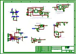
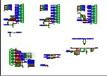
Before powe r-on, please check the board accordi ng to the releva nt block diagram and circuit
diagram, and make sure that no serious issue or mistake can destroy the board. For e xample, the
output of DC/DC and LDO should not be shorted to ground.
Supply a suited voltage and power-on, then check the voltage according to the relevant block
diagram, circuit diagram and voltage spec. The error should less than 5%. For example, the voltage
for main chip (+3V3, AV3.3, +1V2, CORE1V2, etc.), the voltage for DDR (DDRV), the voltage for
amplifier (AMP_VCC), etc...
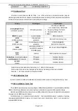
Position
Value
Remark
UD90
5V
±
5%
UD60
1.15V
±
5%
U17
2
/U17
5
3.3V
±
5%
U174
1.5V
±
5%
U201 TUNER_3.3V
1.2. SW Image download
(
Developing
)
Download the latest release SW from below PDM system:
- Link: http://sw.tcl-cctv.com
- Username:
- Password:
See Appendix
o
“How to upgrade FLASH SW using USB”
1.3. Project ID Modification
There are different ID stored into the NVM depending on dif ferent Panels settings and Models
features, but there’s only one key branching Project ID that includes all. So, it’s not recommended to
modify Panel ID with Hyper terminal as other ID features may not change!
To modify Project ID, you need to go through “
Design menu
Æ
Service menu
Æ
Project ID
”, then
spin left or right with RCU “
Zoom±
” keys to suitable ID (Project name is dynamically refreshed).
See Appendix
p
“
How to change Project ID with RCU
”
Here below is none exhaustive Project ID table for reference:
MODEL
ProjectID
Panel Name
L
28B2500
001
LVW320NEAL CJ9W02
L
32B2800
002
LVF400NEAL SJ9W00 V6
L
40B3800
005
LVF480ND2L CD9W00 V3
Summary of Contents for L40B2800
Page 32: ......


