background image

<Document ID>

© NXP B.V. 2007. All rights reserved.

Product data sheet

Rev. 0.11 — 25 January 2007 

2 of 230

NXP Semiconductors

UOC-TOP-64 N1 series

Signal processor for CRT TV

2.

Features

2.1 Analog Video Processing

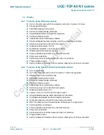
2.1.1 Overview of available features (AV-110/90 and Mono-110 concept)

„

Multi-standard vision IF circuit with alignment-free PLL demodulator

„

Internal (switchable) time-constant for the IF-AGC circuit

„

Switchable group delay correction and sound trap (with switchable centre frequency) 
for the demodulated CVBS signal

„

Separate Second Sound IF output or FM demodulator output without de-emphasis 
available, which can be used as input for an external BTSC decoder or as input for 
external sound band-pass filter for second language processing.

„

Separate SSIF input available as input for the FM-PLL demodulator to demodulate 
FM-radio with an IF frequency of 10.7 MHz, or as input from an external sound 
band-pass filter for second language processing.

„

AM demodulator without extra reference circuit

„

The mono intercarrier sound circuit has a selective FM-PLL demodulator which can be 
switched to the different FM sound frequencies (4.5/5.5/6.0/6.5 MHz). The quality of 
this system is such that the external band-pass filters can be omitted. 

„

The FM-PLL demodulator can be set to centre frequencies of 4.72/5.74 MHz so that a 
second sound channel can be demodulated. In such an application it is necessary that 
an external bandpass filter is inserted. 

„

Audio switch circuit with 2 stereo inputs (1 stereo input can also be switched into two 
mono sound inputs) and a stereo output which can be used for the drive of for audio 
power amplifiers (with volume and tone-control) or as SCART/CINCH output. The 
second stereo input is only available via the combined C2/C3/C4/AUDIOIN5R pin for 
the right channel and via the combined CVBS4/Y4/AUDIOIN5L pin for the left channel.

„

Video switch with 3 external CVBS inputs. All CVBS inputs can be used as Y-input for 
Y/C signals. However, only 1 Y/C source can be selected because the circuit has 1 
chroma input. CVBS3/Y3 input available in combination with the G/Y-3 input pin.

„

1 CVBS output, this output can be used as monitor video output or as front-end video 
output or as independent selectable video output. 

„

Automatic Y/C signal detector.

„

Integrated luminance delay line with adjustable delay time

„

Only one reference (24.576 MHz) crystal required for the m-Controller, Teletext- and 
the color decoder 

„

Multi-standard color decoder with automatic search system and various “forced mode” 
possibilities

„

Internal base-band delay line

„

Indication of the Signal-to-Noise ratio of the incoming CVBS signal

„

Linear RGB/YP

B

P

R

 input. 

„

Scan Velocity Modulation output. The SVM circuit is active for all the incoming CVBS, 
Y/C and RGB/YP

B

P

R

 signals. The SVM output is combined with the black current input 

of the black current stabilisation circuit. By means of a small application adaptation 
both functions can be operational in parallel.

Summary of Contents for NX56LA

Page 1: ...troduction 26 6 PCB Layout 33 7 Schematic Diagram 35 8 Specification of Main IC 40 9 BOM list Temporal lacking 61 10 Explode View Diagram Temporal lacking 74 This manual is the latest at the time of p...

Page 2: ...of uninsulated voltage within the products enclosure that may be of sufficient magnitude to constitute a risk of electric shock to the person The exclamation point within an equilateral triangle is i...

Page 3: ...nnel 8 Do not subject your television set to impact of any kind Be particularly careful not to damage the picture tube surface 9 Unplug this television set from the wall outlet before cleaning Do not...

Page 4: ...porting structure grounding of the lead in wire to an antenna discharge unit size of grounding conductors location of antenna discharge unit connection to grounding electrode and requirements for the...

Page 5: ...21 If you are unable to restorenormal operation by following the detailedprocedurein your operating instructions do not attempt any further adjustment Unplug the set and call your dealer or service te...

Page 6: ...TCL Thomson Electronics R D Center Shen Zhen Lab Chassis Name Serial No Issued On Page Updated On Version Product Functional Specification NX56 LA 2008 5 19 1 of 7 1 0...

Page 7: ...be reproduced or copied or used as the basis for the manufacture or sale of apparatus or devices without the written permission of TCL Thomson Electronics Version Information Version states by two Ar...

Page 8: ...Checked by Released by Prepared by lipeng 2008 5 19 Checked by Released by Revised by Checked by Released by Revised by Checked by Released by Chassis Name Issued On Updated On 3 of 7 29185 V1 0 03 B1...

Page 9: ...de Screen Switching Comb filter Picture Enhancement LTI CTI Black Stretch Dynamic Skin Others Picture Control General Brightness X X Sharpness X X Contrast X X Tint X X Color X X Picture Control Speci...

Page 10: ...lish Portugal Espanol English Portugal Espanol Features General AT Biological Clock Calendar Clock Channel Swap X X Channel Naming Child Lock X X Favorite Channel X X Game Hotel Mode X X High Sensitiv...

Page 11: ...BS Component In YPbPr Cinch for 50Hz In Y C Cinch CVBS Stereo 1 1 1 2 In Y C Cinch CVBS Mono In Cinch CVBS Stereo In Cinch CVBS Mono Out Cinch CVBS Stereo Out Cinch CVBS Mono 1 follow TV 1 follow TV Y...

Page 12: ...U Indication on BACKOVER Made in in family sheet FCC Elect Shock Caution Label CE Elect Shock Caution Label Warning Label Others Miscellaneous Mains Voltage 100 240V 100 240V Mains Frequency 50 60Hz 5...

Page 13: ...TCL THOMSON Electronics R D Center Shen Zhen Lab Chassis Name NX56 LA Serial No Issued on 2008 05 19 Page Page 1 of 12 Updated on Version 1 0 NX56 LA Chassis Alignment Procedure...

Page 14: ...ns are the property of TCL Thomson Electronics and shall not be reproduced or copied or used as the basis for the manufacture or sale of apparatus or devices without the written permission of TCL Thom...

Page 15: ...story Model No Status Date Comment Prepared by LIPENG 2008 05 15 Checked by 29185 Released by 03 B185SAE SC31 29185 NX56 LA Prepared by LIPENG 2008 05 15 Checked by 21M63US Released by 03 DM62SAE SC31...

Page 16: ...HOTKEY had set to ON 1 the set will enter the P Mode automatically 1 2 Exit the P Mode Press the RECALL or MENU key on RC to exit the P Mode 1 3 Keys function on RC at the P Mode Use the RC to naviga...

Page 17: ...ng for chassis RF AGC adjustment Parameter setup White balance Adjustment Aging Adjustment of focus voltage Adjustment of screen voltaget PAL geometry adjustment NTSC geometry adjustment Set shopping...

Page 18: ...ant connectors and modules must be connected and inserted 2 Main voltage is at 220VAC 50Hz voltage range 110VAC 240VAC 50Hz 3 Connect a voltmeter to B Cathode of D808 and switch on the set 4 Input Phi...

Page 19: ...litude B Enter P Mode press 6 key on RC to select AGCT C Adjust the AGCT value until the hint display AGC just change between 0 and 1 3 3 Screen Focus adjustment Notes Alignment below should be done a...

Page 20: ...or YUV mode when production but the BLOR Y BLOG Y and BLOB Y items which locate in EEPROM address 0x0A 0x0B and 0x0C need to write in the right values to set the YUV mode black level offset before pro...

Page 21: ...al 3 On producing please use the AUTO OFFSET On page 2 function to easy the geometry adjustment of NTSC signal When finished the PAL signal geometry adjustment press 2 key to enter page 2 to select AU...

Page 22: ...d option 1 Enter P Mode press key 4 to select page 4 Set the corresponding item to require value See below table 3 6 1 for detailed description Table 3 6 1 Producing parameter setup and option page 4...

Page 23: ...etry adjustment When finished the PAL geometry adjustment trigger the AUTO OFFSET from 0 to 1 then the geometry adjustment of NTSC signal will finish automated If now the geometry of NTSC signal is lo...

Page 24: ...ELAY 2 CC s position Don t adjust 5 Enter P Mode press key 8 to select page 8 Set the corresponding item to require value See below table 3 6 5 for detailed description Table 3 6 5 Producing parameter...

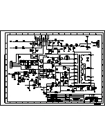
Page 25: ...Coupler IC803 R G B P201 Tuner TU101 IF AMP Q101 SAW Z2O1 Pin44 46 V AMP IC301 STV8172A Pin14 15 VDA B SCA SDL EEPROM IC001 Pin 56 H OUT H Driver AMP Q401 Q402 P901 TV AV SV B FBT T401 200V 24V 6 3V...

Page 26: ...fferent UOC The UOC for Latin America have CCD Chip and BTSC function so added AN5832SA to realize BTSC but the UOC for Asia Pacific region does not have the two functions but SECAM system is necessar...

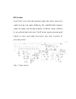
Page 27: ...nd signal amplifying The amplified high frequency signal accompany with the high frequency oscillation voltage oscillated by set oscillator input to the mixer The IF picture signal and sound signal fo...

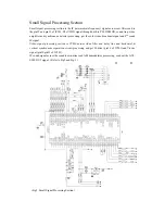
Page 28: ...processing get the color video broadcast signal and 2nd sound IF signal Video signal processing section is CVBS across video filter and delay line and horizontal vertical synchronous separation circu...

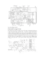
Page 29: ...ng in switch on and off situation get good linearly and enough amplitude of saw tooth wave current to drive horizontal deflection yoke scanning L456 is horizontal width coil and L458 is horizontal lin...

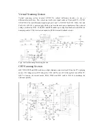
Page 30: ...r transformer Pin 6 is boost voltage rectified by D301 C309 C301 and R305 makes up a voltage feedback network R306 is a damping resistor C306 is correction capacitor R308 is current feedback resistor...

Page 31: ...LF801A and CX802 makes up a differential mode rejection LF802 and CY801 CY802 makes up a common mode rejection network D801 D804 is rectifying network 300Vdc voltage supply pin3 of T801 also through...

Page 32: ......

Page 33: ......

Page 34: ......

Page 35: ......

Page 36: ......

Page 37: ......

Page 38: ...1I567...

Page 39: ......

Page 40: ...ot contain an East West and Scan Velocity Modulation SVM output This concept is intended for 90 picture tubes Mono 110 concept The functional content of this concept is comparable with that of the AV...

Page 41: ...pplication it is necessary that an external bandpass filter is inserted Audio switch circuit with 2 stereo inputs 1 stereo input can also be switched into two mono sound inputs and a stereo output whi...

Page 42: ...tion with two control loops and alignment free horizontal oscillator Vertical count down circuit Vertical driver optimized for DC coupled vertical output stages Horizontal and vertical geometry proces...

Page 43: ...ing 8 bit A D converter with 4 multiplexed inputs 4 PWM 6 bits outputs for analogue control functions 2 3 Data Capture Teletext and Closed Caption devices Text memory for 1 page Inventory of transmitt...

Page 44: ...f coloration Programmable Cursor Special Graphics Characters with two planes allowing four colors per character 2 4 2 Features of the Teletext and Closed Caption devices Four character sets Up to 576...

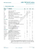
Page 45: ...A IPAudio supply current 8 0 V AV 110 90 and mono 110 version 10 mA Ptot total power dissipation 1 1 W Input voltages ViVIFrms video IF amplifier sensitivity RMS value 75 150 V ViSSIF rms sound IF amp...

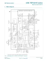
Page 46: ...AL GEOMETRY EAST WEST AGCOUT VIFIN C2 C3 C4 CVBS4 Y4 H OUT PEAKING SCAN VELOCITY RGB YP R P B CON BRI RO GO BO BLKIN RGB CONTROL OSD TEXT INSERT WHITE P ADJ CONTR BRIGHTN RGB MATRIX H V REF Y DELAY AD...

Page 47: ...OUT VIFIN H OUT RGB YP R P B CON BRI RO GO BO BLKIN VGUARD RGB CONTROL OSD TEXT INSERT CCC BLACK ADJ WHITE P ADJ CONTR BRIGHTN RGB MATRIX H V REF Y DELAY ADJ SATURATION CVBS2 Y2 YSYNC IFVO SVO SOUND P...

Page 48: ...output AVL capacitor AVL 16 16 AVL capacitor DECBG 17 17 17 bandgap decoupling SECPLL 18 18 18 SECAM PLL decoupling GND1 19 19 19 ground 1 for TV processor PH1LF 20 20 20 phase 1 filter PH2LF 21 21 2...

Page 49: ...GO 45 Green output RO PROUT 46 46 Red output PR output RO 46 Red output BLKIN VGUARD SVM 1 6 47 black current input vertical guard scan velocity modulation output BLKIN VGUARD 1 6 47 47 black current...

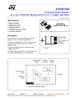
Page 50: ...onitor applications This device supplied with up to 35 V provides up to 2 5 App output current to drive the vertical deflection yoke The internal flyback generator delivers flyback voltages up to 75 V...

Page 51: ...e of either VS 2 or 40 volts 2 Thermal Data Symbol Parameter Value Unit Voltage VS Supply Voltage pin 2 Note 1 and Note 2 40 V V5 V6 Flyback Peak Voltage Note 2 70 V V3 Voltage at Pin 3 Note 2 Note 3...

Page 52: ...put I1 Input Bias Current V1 1 V V7 2 2 V 0 6 1 5 A 1 I7 Input Bias Current V1 2 2 V V7 1 V 0 6 1 5 A VIR Operating Input Voltage Range 0 VS 2 V VI0 Offset Voltage 2 mV DVI0 dt Offset Drift versus Tem...

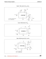
Page 53: ...2 and I6 Figure 2 Measurement of V5H Figure 3 Measurement of V3L and V5L 1V a 39kW 5 1 b I1 a I2 and I6 measurement b I1 measurement S Vs 2 6 I2 I6 4 7 2 2V STV8172A 5 6kW I5 5 1V 7 2 2V 1 4 Vs 2 6 V5...

Page 54: ...OFF the positive supply alone In this state where both inputs are the same voltage as pin 2 or higher the output will sink negligible current from the deviation coil 4 1 1 Application Hints For calcul...

Page 55: ...tion of any ripple caused by a voltage drop in the ground see Figure 5 if you manage to apply the same fraction of ripple voltage to both booster inputs For that purpose arrange an intermediate point...

Page 56: ...of the yoke 4 2 1 Application Hints Gain is defined as in the previous case Choose R1 then either R2 or R3 For good output centering V7 must fulfill the following equation or Figure 6 AC coupled Appl...

Page 57: ...is the common mode current at peak of signal i icm ip and i icm ip therefore the peak differential signal is ip ip 2 ip and the peak peak differential signal 4ip The application is described in Figure...

Page 58: ......

Page 59: ......

Page 60: ......

Reviews: