Test and Alignment Specification for RT2841 Series (v0.01).docx
Page 5 of 27
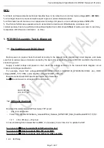
INFO:
All tests and measurements mentioned hereafter have to be carried out at a normal mains voltage (
220 ~ 240 VAC
)
All voltages have to be measured with respect to ground, unless otherwise stated
All final tests have to be done on a complete set including LCD panel in a room with temperature of
25+/-7°C
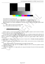
The Picture Performance assessment such as Gamma Correction and White Balance (luminance and
colortemperature) has to be performed into subdued lighted room after at least
45min
of warm-up in order to avoid any
temperature drift influence (colorimetric vs. time)
1. PCB/SKD Assembly: Test & Alignment
1.1.
Pre-Conditions and DC/DC Check
Before power-on, please check the board according to the relevant block diagram and circuit diagram, and make
sure that no serious issue or mistake can destroy the board. For example, the output of DC/DC and LDO should not be
shorted to ground.
Supply a suited voltage and power-on, then check the voltage according to the relevant block diagram, circuit
diagram and voltage specification.
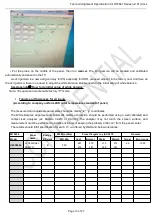
For example, check SoC voltage(AVDD3V3,DVDD3V3,VCCK_1V0,AVDD1V0_STB,095VM,3V3SB, etc.), DDR
voltage (DDRV_1V5,1V5M) , audio amplifier voltage(24V AMP_VCC),etc...
Measurements should fulfill specification within ±5% tolerances.
Note
①:
See enclosed circuit diagram for more details.
40-RT41K1-TEB
2HG 05-07.pdf
1.2.
SW Image download
Download the latest release SW from below FTP server:
-
Link: \\10.120.99.200\
-
Folder: \\10.120.99.200\Software_release\Official_Release_SW\NPI\SW_SQA_Pass\Reartek\RTK
外销机芯
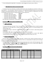
1.2.1
LR or PR step. ---Only test
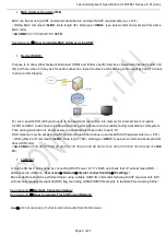
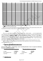
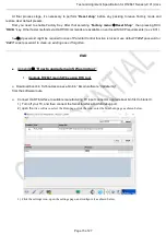
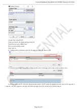
In case of starting from blanked flash / eMMC, it’s necessary to use “rtice tool” to update the SW.
See Appendix
⑴
“
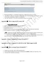
How to upgrade Main SW using rtice tool
”
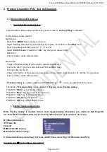
See Appendix
⑵
“How to upgrade Main SW using USB”
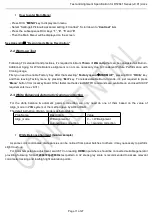
See Appendix
⑶
“How to upgrade main SW using USB and RCU”
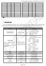
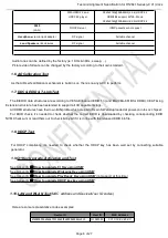
1.2.2
MP Step
Summary of Contents for RT41VS-EU
Page 32: ...Test and Alignment Specification for RT2841 Series v0 01 docx Page 27 of 27...
Page 33: ...11 Oct 18 Page 8 nRT41 Chassis Block Diagram...
Page 34: ...11 Oct 18 Page 9 nPower supply Block Diagram...
Page 35: ...11 Oct 18 Page 10 nRT41 Power supply Block Diagram...
Page 46: ...11 Oct 18 Page 23 nTrouble Shooting...
Page 47: ...nTrouble Shooting 11 Oct 18 Page 24...
Page 48: ...nTrouble Shooting 11 Oct 18 Page 25...
Page 49: ...11 Oct 18 Page 11 nKey Test Point Main Power Supply 12V 12V Test point...
Page 51: ...11 Oct 18 Page 13 nKey Test Point LDC1 1V5_DDR UDC1 3V3_STB to 1V5_DDR 3V3_STB STR Enable...
Page 52: ...11 Oct 18 Page 14 LDB1 CORE 1V0 nKey Test Point 12V UDDB 12V TO 1V0...
Page 53: ...11 Oct 18 Page 15 LDA1 5V nKey Test Point UDA1 12V TO 5V...
Page 57: ...11 Oct 18 Page 19 nKey Test Point PANEL_VCC 12V Q900 PANEL_VCC...
Page 58: ...11 Oct 18 Page 20 Main Chip 1 SOC Config 2 24MHz CRYSTAL nKey Test Point Test Point...

