21
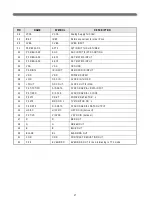
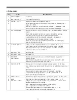
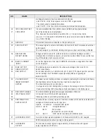
4. Pin Description
N O
N A M E
D E S CR IPTIO N
1
SO U N D IF IN PU T
SIF IN PU T
2
EXT AU D IO IN PU T
EXTER N AL AU D IO IN PU T
3
4
VC O R EF FILTER
The IF V C O tuned circuit is applied to these pin.
Its resonance frequency m ust be tw o tim es the if-frequency and in betw een a
range of 64-120M hz.
This range is suitable for the if standards as 33.4,38.9,45.75 and 58.75 M H z.
The VC O freq. can be adjusted by IIC bus so a fixed coil can be used.
5
PLL LO O P FILTER
The PLL loopfilter is a first order filter w ith R =390 ohm and C =100nF in series to
ground.
The loopfilter bandw idth is 60KH z and is optim al for both fast catching
and sufficient video suppression for optim al sound perform ance.
Sound perform ance can theoretically be im proved by adding a sm all
capacitor(approx.0-4.7nF) betw een pin 5 and ground.
This how ever m ust be evaluated further because the norm al video signal
response should not be effected.
6
IF VID E O O U TPU T
Although the video output im pedance is low it is recom m ended to avoid
high frequency current in the output due to for instance sound trap filters.
This can be achieved by m eans of an em itter follow er at the video output
w ith a 1
resistor in series w ith the base.
7
BU S IN PU T : SC L
serial clock line
8
BU S IN PU T : SD A
serial data line
9
BAN D G AP
D EC O U PLIN G
The bandgap circuit provides a very stable and tem perature ijdependent
reference voltage.
This reference voltage(6.7V)ensures optim al perform ance of the TD A8374
and is used in alm ost all functional circuit blocks.
10
C H R O M A IN PU T
The supplied C S -VH S input burst am plitude should be nom inally 300
pp.
(assum ed is a colour bar signa! w ith 75% saturation and w ith chrom a/burst ratio of
2.2/1).
The C S-VH S input is internally clam ped to 4V via 50
.
The external AC coupling capacitor w ith 50* form s a high pass filter.
A recom m ended coupling capacitor is 1 nF ; the high pass filter cut off
frequency is then approxim ately 3kH z.
11
Y/C VBS IN PU T
The Y S-VH S signal of 1Vpp (inclusive sync am plitude) is AC coupled to pin11.
12
37
M AIN
PO SITIVE SU PPLY
The TD A8374A has a m ain supply pin 12 and a hprizontal supply pin 37.
Both pins have to be supplied sim ultaneously. N otice that the IC has not been
designed to use this pin 37as start pin.
(pin 37 supplies the horizontal oscillator, PH I-1 and PH I-2)
(pin 12 supplies the rest of the circuits in th IC )
The nom inal supply voltage is 8V. W ith m in/m ax values of 7.2-8.8V.
Also in stand-by condition th IC m ust be supplied w ith 8V.
Summary of Contents for MV1421
Page 1: ...SERVICE MANUAL MV1421 1422 4822 34cm 48cm Televideo Effective December 1999 MV4822SERV ...
Page 6: ...4 3 BLOCK DIAGRAM 3 1 Audio Signal Flow ...
Page 7: ...5 3 2 Video Signal Flow ...
Page 8: ...6 3 3 TV and monitor power switching ...
Page 22: ...20 3 Block Diagram ...
Page 53: ......
Page 54: ......
Page 55: ......
Page 117: ...2 Main PCB Assy Circuit Diagram SECTION BEFORE AFTER MAIN TUNER ...
Page 118: ...3 SECTION BEFORE AFTER SUB TUNER ...
Page 125: ...10 Exploded View MV1421 model ...
Page 126: ...11 Exploded View MV1422 model ...
Page 127: ...12 Exploded View MV4822 model ...
Page 128: ...13 Exploded View DVT 20F9 model ...
Page 129: ...14 Exploded View DVT 21F1 model ...
Page 130: ...15 Exploded View DVT 21F2 model ...


