background image

11.1 IC701 (M38503M2404F) : Micro Computer

TOP


PREVIOUS


NEXT


Pin No.

Name

I/O

Function

1

VCC

I

Power supply (+5 V) terminal

2

VREF

I

Reference voltage input

3

AGND

-

GND terminal

4

CS

I

Chip select signal input

5

NC

-

Not used, open

6

REMCON

I

Remote control signal input

7

BACKUP

I

Power failure detect signal input

8

NC

-

Not used, open

9

SELDATA

O

Data signal output for input select IC (IC201 and IC202)

10

SELCLK

O

Clock signal output for input select IC (IC201 and IC202)

11

SELSTB

O

Strobe signal output for input select IC (IC201 and IC202)

12

POWERSW

I

Selector switch (S804) detect signal input

13

LEDCLK

O

Clock signal output for LED drive IC

14

LEDDATA

O

Data signal output for LED drive IC

15

CNVSS

-

Connected to GND

16

VRDOWN

O

Motor drive signal output (Volume down)

17

VRUP

O

Motor drive signal output (Volume up)

18

RESET

I

System reset signal input

19

XIN

I

Connected to the ceramic oscillator (8 MHz)

20

XOUT

O

Connected to the ceramic oscillator (8 MHz)

21

GND

-

GND terminal

22

BATELED

-

Battery level (empty) LED (D809) drive signal output (Not used, open)

23

BATFLED

-

Battery level (full) LED (D809) drive signal output (Not used, open)

24

VIALED

O

VIA LED drive signal output

25

VGALED

O

VGCA LED drive signal output

26

STABYLED

O

Stand by LED drive signal output

27

FRNTOUT

O

Front output control signal output

28

CSWSOUT

-

Center/S.woofer/Surround output control signal output (Not used, open)

29

PWRRLY

O

Power control signal output

30

CHRGRLY

-

Battery charge relay control signal output (Not used, open)

31

BATRLY

-

Battery drive relay control signal output (Not used, open)

Summary of Contents for SE-A909S

Page 1: ...c Diagram Notes 6 2 Schematic Diagram 7 Printed Circuit Board Diagram 8 Block Diagram 9 Wiring Connection Diagram 10 Measurements and Adjustments 10 1 Measurement instruments and Special tools 10 2 Ou...

Page 2: ...1999 Matsushita Electric Industrial Co Ltd All rights reserved Unauthorized copying and distribution is a violation of law TOP NEXT...

Page 3: ...edures 5 Type Illustration of ICs Transistors and Diodes 6 Schematic Diagram 6 1 Schematic Diagram Notes 6 2 Schematic Diagram 7 Printed Circuit Board Diagram 8 Block Diagram 9 Wiring Connection Diagr...

Page 4: ...12 Replacement Parts List 13 Cabinet Parts Location 14 Packaging PV PV...

Page 5: ...Service Manual TOP NEXT AD9907176C2 Control Amplifier SU C909U Colour K Black Type Area E Europe and Russia...

Page 6: ...1999 Matsushita Electric Industrial Co Ltd All rights reserved Unauthorized copying and distribution is a violation of law TOP NEXT...

Page 7: ...1 Note TOP PREVIOUS NEXT Refer to the servise manual for Model No SE A909S ORDER No AD9907177C2 for information on Accessories Connections Operations and Packaging TOP PREVIOUS NEXT...

Page 8: ...2 Location of Controls TOP PREVIOUS NEXT...

Page 9: ...TOP PREVIOUS NEXT...

Page 10: ...ate on power supplied from the Power Amplifier SE A909S When operating the unit SU C909U alone for testing and servicing without having power supplied from the Power Amplifier SE A909S use the followi...

Page 11: ...t TP2 Shown in Fig 1 2 Connect the DC 12 V to 15 V more than 0 1 A to the point TP5 and the GND terminal to the point TP4 using the DC power supply Shown in Fig 1 3 Connect the DC 12 V to 15 V more th...

Page 12: ...XT 1 Input a signal 1 kHz 100 mV to the each line in terminal 2 Connect the oscilloscope or the speaker with the built in amplifier to the PRE OUT terminals and check if the signals are outputting fro...

Page 13: ...4 Operation Checks and Component Replacement Procedures TOP PREVIOUS NEXT...

Page 14: ......

Page 15: ...TOP PREVIOUS NEXT...

Page 16: ...5 Type Illustration of ICs Transistors and Diodes TOP PREVIOUS NEXT TOP PREVIOUS NEXT...

Page 17: ...6 Schematic Diagram TOP PREVIOUS NEXT 6 1 Schematic Diagram Notes 6 2 Schematic Diagram TOP PREVIOUS NEXT...

Page 18: ...T This schematic diagram may be modified at any time with the development of new technology Notes S801 VGCA switch S802 Tape monitor switch TAPE MONITOR S804 Input select switch SELECTOR S805 Unit on...

Page 19: ...ng on theinternal impedance of the DC circuit tester No mark Power ON Important safety notice Components identified by mark have special characteristics important for safety Furthermore special parts...

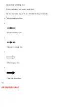
Page 20: ...Put a conductive mat on the work table Do not touch the legs of IC or LSI with the fingers directly Voltage and signal line Positive voltage line Negative voltage line Phono signal line Tape rec sign...

Page 21: ...6 2 Schematic Diagram TOP PREVIOUS NEXT TOP PREVIOUS NEXT...

Page 22: ...7 Printed Circuit Board Diagram TOP PREVIOUS NEXT TOP PREVIOUS NEXT...

Page 23: ...8 Block Diagram TOP PREVIOUS NEXT TOP PREVIOUS NEXT...

Page 24: ...9 Wiring Connection Diagram TOP PREVIOUS NEXT TOP PREVIOUS NEXT...

Page 25: ...10 Measurements and Adjustments TOP PREVIOUS NEXT 10 1 Measurement instruments and Special tools 10 2 Output Voltage Adjustment TOP PREVIOUS NEXT...

Page 26: ...10 1 Measurement instruments and Special tools TOP PREVIOUS NEXT AC electric voltmeter AC EVM AF oscillator TOP PREVIOUS NEXT...

Page 27: ...the input source to CD 3 Connect the measuring instrument as shown in Fig 2 4 Apply 1 kHz 200 mV signal to CD terminal 5 Adjust the VOLUME to maximum 6 Adjust VR311 L ch and VR312 R ch so that the ou...

Page 28: ...TOP PREVIOUS NEXT...

Page 29: ...11 Terminal Function of ICs TOP PREVIOUS NEXT 11 1 IC701 M38503M2404F Micro Computer TOP PREVIOUS NEXT...

Page 30: ...D drive IC 15 CNVSS Connected to GND 16 VRDOWN O Motor drive signal output Volume down 17 VRUP O Motor drive signal output Volume up 18 RESET I System reset signal input 19 XIN I Connected to the cera...

Page 31: ...H Not used open 38 BATLVL2 Battery voltage detection 2 signal input Not used open 39 NC Not used open 40 RSWAD I Power switch S805 detect signal input 41 KEYAD I Tape monitor and VGCA switch input 42...

Page 32: ...uation of this assembly in production the item will continue to be available for a specific period of time The retention period of availabilityis dependent on the type of assembly and in accordance wi...

Page 33: ...4 24 RHD26034 SCREW 3 25 RHN90001 NUT 2 26 RKF0593 Q DOOR 1 27 RKG0009 MAGNET 1 28 RKW0273A K FILTER 1 29 RME0284 SPRING 1 30 RMR1202 K ARM L 1 31 RMR1203 K ARM R 1 32 RMR1204 K MAGNET HOLDER 1 33 RM...

Page 34: ...ECBT1E103ZF 25V 0 01U 1 C251 58 ECBT1H101KB5 50V 100P 8 C301 02 ECBT1H181KB5 50V 180P 2 C303 04 ECBT1E103ZF 25V 0 01U 2 C305 06 ECA1EPXS100B 25V 10U 2 C351 52 ECA1EPXS100B 25V 10U 2 C353 54 ECCR1H101...

Page 35: ...1 C656 ECQV1H104JM3 50V 0 1U 1 C658 ECBT1C103NS5 16V 0 01U 1 C701 02 ECA0JM102 6 3V 1000U 2 C703 RCE1HKAR47BG 50V 0 47U 1 C704 ECEA1HKS2R2 50V 2 2U 1 C705 06 ECBT1C103NS5 16V 0 01U 2 C707 08 RCE1HKAR...

Page 36: ...LR325VCT31 LED 3 D811 SLR325DCT31 LED 1 D812 13 SLR325VCT31 LED 2 D814 15 SLR325DCT31 LED 2 D816 18 SLR325VCT31 LED 3 IC101 AN6558F IC 1 IC201 TC9163N IC 1 IC202 TC9164N IC 1 IC311 UPC4570C IC 1 IC351...

Page 37: ...ISTOR 1 Q502 DTC124EST TRANSISTOR 1 Q521 DTC124EST TRANSISTOR 1 Q522 DTA124ESTP TRANSISTOR 1 Q601 02 DTA124ESTP TRANSISTOR 2 Q603 DTC144ESTP TRANSISTOR 1 Q701 DTC114ESTP TRANSISTOR 1 Q702 DTC114YSTP T...

Page 38: ...ERDS1FJ100 1 2W 10 1 R401 02 ERDS2FJ472 1 4W 4 7K 2 R403 06 ERDS2FJ224 1 4W 220K 4 R407 08 ERDS2FJ392 1 4W 3 9K 2 R409 10 ERDS2FJ102 1 4W 1K 2 R411 12 ERDS2FJ183 1 4W 18K 2 R413 14 ERDS2FJ392 1 4W 3...

Page 39: ...2 ERDS2FJ561 1 4W 560 1 R813 14 ERDS2FJ181 1 4W 180 2 R815 ERDS2FJ331 1 4W 330 1 R819 ERDS2FJ271 1 4W 270 1 R820 ERDS2FJ223 1 4W 22K 1 R821 ERDS2FJ123 1 4W 12K 1 R822 ERDS2FJ331 1 4W 330 1 R823 ERDS2F...

Page 40: ...R311 12 EVNDXAA00B23 VR OUTPUT VOLT ADJ 2 VR401 EVJ02QF01G15 VR BALANCE 1 VR402 03 EVJYA1F01C15 VR BASS TREBLE 2 X701 RSXY8M00D01T OSCILLATOR 1 Z801 RCD12042TH COMPONENT COMBINATION 1 TOP PREVIOUS NEX...

Page 41: ...13 Cabinet Parts Location TOP PREVIOUS NEXT TOP PREVIOUS NEXT...

Page 42: ...14 Packaging TOP PREVIOUS TOP PREVIOUS...

Page 43: ......

Page 44: ......

Page 45: ......

Page 46: ......

Page 47: ......

Page 48: ......

Page 49: ...8 1 8 3 1 RED BLACK 3 1 3 1 BLACK RED CN301 A MAIN P C B W301 C VOLUME P C B D LED P C B E OPERATION P C B B TONE P C B F POWER SWITCH P C B G SELECTOR P C B TAPE1 PRE OUT PHONO TUNER CD DVD TO POWER...

Page 50: ...302 1 2 3 4 5 6 7 1 2 3 4 5 6 7 8 9 18 17 15 16 22 21 19 11 12 14 13 10 20 25 24 23 28 27 26 IC201 1 2 3 4 5 6 7 8 9 18 17 15 16 22 21 19 11 12 1413 10 20 25 24 23 28 27 26 IC202 J J J J J J J J J J J...

Page 51: ...Q601 B C E Q602 B C E Q603 B C E Q710 B C E Q702 JJ J J J J J C303 C304 J D601 2 3 4 5 6 7 8 IC351 1 2 3 4 5 6 7 8 IC511 1 2 3 4 5 6 7 8 IC311 1 RL521 J J J J J J J J J J J J J J J J J C355 C351 C362...

Page 52: ...258 R301 R302 R315 R316 R351 Ref No Lo No R352 R353 R354 R355 R356 R357 R358 R503 R504 R513 R514 R515 R516 R521 R522 R523 R524 R525 R526 R655 R656 R701 R702 R703 R704 R705 Ref No Lo No R706 R707 R708...

Page 53: ...03 R804 R811 L801 R801 R809 SELECTOR P C B G S804 SELECTOR REP2841D S 1 2 3 4 5 6 1 2 3 4 5 6 ELECTRICAL PARTS LOCATION IC801 D801 D802 D803 D804 D806 D807 5B 7A 6A 6A 5A 5A 4A 4A 5B 8A 2A 4A 2A 7A 4A...

Page 54: ...24 0 01 C122 0 01 C117 35V4 7 R129 56K R131 1K C119 4700P C113 6800P R125 12K R127 180K C115 0 022 R123 68 C123 1000P C107 10V33 R117 180 R105 56K R118 180 R106 56K C108 10V33 C124 1000P R124 68 C116...

Page 55: ...124ESTP RELAY DRIVE 5 6 7 8 4 3 2 1 C A B A B C519 25V10 IC511 UPC4570C OUTPUT AMP R515 220K C515 100P R513 100K R514 100K C516 100P R516 220K C514 50V1 C513 50V1 C520 25V10 C301 180P C304 0 01 IC311...

Page 56: ...413 3 9K R411 18K C421 0 082 C423 0 015 C424 0 015 C425 120P R415 22K C415 2200P R407 3 9K C416 2200P R408 3 9K R416 22K C426 120P R410 1K R409 1K C419 3300P C417 0 015 C418 0 015 C420 3300P VR403 2 1...

Page 57: ...3 2 16 15 14 13 12 11 10 Vss DATA CLK Q0 Q1 Q2 Q3 Q4 V DD Q11 Q10 Q9 Q8 Q7 Q5 Q6 1 2 3 4 5 6 7 8 9 1 2 3 1 7 3 2 4 5 6 7 1 3 2 4 5 6 8 R827 100 R826 100 A B C A B C W705A C801 6 3V100 R825 330 D818 L8...

Page 58: ...00 C706 0 01 10K 10K R708 100K R707 100K R728 100K D712 MA165TA C704 50V2 2 6 5 7 8 4 3 2 1 MAIN CIRCUIT A R705 100K D658 MA4056MTA D709 MA165TA D706 MA165TA D710 MA165TA 47K 10K R656 10K D707 MA165TA...

Page 59: ...B3 D701 D702 D704 D705 7 BACKUP CS 4 S805 UNIT ON OFF POWER SW 12 4 6 8 15 D801 808 817 PHONO TUNER CD DVD AUX TAPE1 TAPE MD SOURCE BU2090AFE2 IC801 LED DRIVE B3 16 3 13 LED CLK 14 LED DATA 2 3 AGND...

Page 60: ...amp Logic 2 5 8 3 1 VR DOWN VR UP VR301 VOLUME LOGIC GND 7 JK801 6 5 4 3 2 1 PRE GND AC BACKUP P ON OFF B VIRTUAL D651 652 655 656 M5F78M05L IC601 Regulator To POWER AMPLIFIER SE A909S D707 D706 D710...

Page 61: ...42PIN No 1 BA6218 O G I 9 1 DTC114ESTP DTC114YSTP DTA124ESTP DTC124ESTP DTC144ESTP E C B RL1N4003N02 A Ca Anode Cathode MA165TA MA167TA Anode Cathode A Ca Anode Cathode 1SS291TA A Ca A Ca A Ca SLR325D...

Reviews: