background image

8. Self Check Function

This unit is equipped with a self check function which can detect a part of 
malfunction. Use this function before servicing the unit and check the item as shown 
below.

8.1. Setting to the Self Check Function

1. Turn the power on.

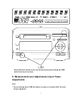
2. Press and hold the STOP button for at least 2 seconds, and while still pressing the 

STOP button, press the REV. SEARCH button for at least 2 seconds. Then the unit 
enters Self Check Function. (Refer to 

Fig.3

.)

Fig.3

8.2. Checking the operation switches

1. When the unit enters the Self Check Function, the FL display turn off.

2. Press the buttons on the unit except the INPUT SELECTOR button, it displays “-” 

mark adapted each buttons.
(

Fig.4

 and 

Fig.5

 is shown about a allotment.)

17

Summary of Contents for SJ-HD501

Page 1: ...AD9907180C2 Mini Disc Deck SJ HD501 Mechanism unit MR3A RAJ3402 Mechanism Series Colour N Gold Type Areas EG Europe EB Great Britain This product is option for systems of SC HD301 and SC HD501 SPECIFI...

Page 2: ...PLAY 90dB Wow and flutter Below measurable limit Input Analog input Level impedance 500mV 47k Digital input Optical in 1 Optical in 2 Wavelength 660nm Output Analog output Level impedance 2 0V 600 Ge...

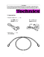
Page 3: ...1 Accessories AC power supply cord 1pc Optical cable 1pc RJL1X001B05D 3...

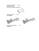
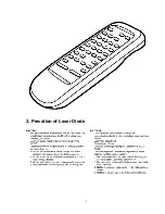
Page 4: ...Remote control batteries 2pcs R6 LR6 AA UM 3 Note These are available on sales route Stereo phono cables 2pcs RJL2P004B08 Remote control transmitter 1pc EUR645272 4...

Page 5: ...2 Precation of Laser Diode 5...

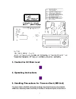
Page 6: ...erating Instructions 5 Handling Precautions for Traverse Deck MD Unit The laser diode in the MD unit optical pickup may break down due to potential difference caused by static electricity of clothes o...

Page 7: ...ort land between the No 25 LD GND and No 24 LD pins on the flexible board is shorted with a solder build up to prevent damage to the laser diode As shown in Fig 1 To connect to the PC board be sure to...

Page 8: ...Fig 2 2 Work table grounding Put a conductive material sheet or steel sheet on the area where the optical pickup is placed and ground the sheet Caution The static electricity of your clothes will not...

Page 9: ...Procedures 9...

Page 10: ...10...

Page 11: ...11...

Page 12: ...12...

Page 13: ...13...

Page 14: ...14...

Page 15: ...s displayed if any For details of the error codes refer to Fig 2 In the case of no errors is displayed on FL 3 If more than one error exists the display will sequentially show the respective error cod...

Page 16: ...Fig 2 16...

Page 17: ...nd hold the STOP button for at least 2 seconds and while still pressing the STOP button press the REV SEARCH button for at least 2 seconds Then the unit enters Self Check Function Refer to Fig 3 Fig 3...

Page 18: ...5 8 3 Checking the FL display 1 Press the INPUT SELECTOR button 2 All buttons works normally except the POWER button FL display and LED turns on and off at 0 5 second interval Refer to Fig 6 and Fig 7...

Page 19: ...n be canceled by pressing and holding the STOP button for at least 2 seconds 9 Measurements and Adjustments Laser Power Adjustment Note If you exchange parts of MD unit when you repair you must perfor...

Page 20: ...st disc Pre mastered disc RFKV0006 or RFKV0014 Recordable disc available on sales route with music recorded Insulated driver for adjustment such as a ceramic driver Remote control transmitter 9 2 Set...

Page 21: ...22 too firmly If the screw is tightened too much to deform the resin the position of the head is moved and this affects its recording operation Recommended torque for mounting screw 700 g cm 100 g cm...

Page 22: ...te power to even momentarily reach or exceed 5 5 mW Doing so will result in damage to the optical pickup Do not set the unit to the laser power adjustment mode with the MD loaded Doing so may result i...

Page 23: ...mechanism Refer to Fig 11 Caution Do not allow the laser power meter to come in contact with either the optical pickup or the magnetic head Fig 10 Fig 11 23...

Page 24: ...ading of the laser power meter or cartridge type laser power meter is within the specified If it is not within the specified range adjust by turning VR1 Refer to Fig 12 Specified range read power 600...

Page 25: ...0 1mW Caution Do not allow the write power to even momentarily reach or exceed 5 5mW Doing so will result in damage to the optical pickup 7 Press 3 on the player s remote control ROM LASER will be dis...

Page 26: ...ithin the specified range first switch off the power and then reset the unit to the adjustment mode and repeat the adjustment procedure 10 Troubleshooting Guide Please refer to this Troubleshooting Gu...

Page 27: ...27...

Page 28: ...28...

Page 29: ...29...

Page 30: ...30...

Page 31: ...31...

Page 32: ...32...

Page 33: ...33...

Page 34: ...11 Schematic Diagram Notes 11 1 Schemtic Diagram Notes This schematic diagram may be modified at any time with the development of new technology Notes S1 PROTECT det switch 34...

Page 35: ...LECTOR switch S903 Skip Search switch S904 Skip Search switch S905 Edit EDIT switch S906 Enter ENTER switch S907 Track mark mode select character skip TRACK MARKING CHARA SKIP S908 Display mode select...

Page 36: ...safety Furthermore special parts which have purpose of fire retardant resistors high quality sound capacitors low noise resistors etc are used When replacing any of components be sure to use only man...

Page 37: ...12 Schematic Diagram 13 Printed Circuit Board 14 Block Diagram 15 Wiring Connection Diagram 16 Terminal Function of IC s 16 1 IC1 AN8772FHQ RF AMP 37...

Page 38: ...E O Tracking error signal output terminal 12 CRS IN I Track cross input terminal 13 TGAIN I Tracking gain adjustment input terminal 14 LNP O Lens position signal output terminal 15 AB GAIN I APP compe...

Page 39: ...ction terminal 34 EQ IN I EQ input terminal 35 ARFO O RF amp output terminal 36 SVREF I Reference voltage input terminal 37 VREF O Reference voltage output terminal 38 RF1 I RF1 signal input terminal...

Page 40: ...10 PGND2 GND terminal 11 VO4 O Tracking coil driver output terminal 12 VO4 O Tracking coil driver output terminal 13 VO3 O Focus coil driver output terminal 14 VO3 O Focus coil driver output terminal...

Page 41: ...nal 5 AS I AS signal input terminal 6 DRMONI I Drive voltage monitor input terminal 7 BAT I Battery power supply terminal Not used connected to GND 8 AMONI Servo analog monitor signal output Not used...

Page 42: ...0 Power supply terminal for I O pad 29 DVss0 GND terminal 30 32 RAD12 RAD10 DRAM address output terminal Not used open 33 42 RAD9 RAD0 O DRAM address output terminal 43 46 RDT3 RDT0 I O DRAM data inpu...

Page 43: ...nnected to GND 68 DATA I CD data input terminal Connected to GND 69 TX O Digital audio interface signal output terminal Not used open 70 RX1 I Digital audio interface signal 1 input terminal 71 RX2 I...

Page 44: ...nal 89 NRFLD O RF serial load output terminal 90 TRCRS I Track cross input terminal 91 OFTR I Off track signal input terminal 92 APCD O Laser power PWM output terminal 93 EXEFMCK I External FM clock i...

Page 45: ...minal 10 NEFMON O Magnetic head current output terminal 11 TEST01 O Test signal output terminal Not used open 12 TVSW I Traverse innermost detection switch signal input terminal 13 DISC IN I Disc dete...

Page 46: ...20 MMOD Connected to GND 46...

Page 47: ...Test signal output terminal Not used open 31 VDD2 3V I Power supply terminal 3V 32 OSC1 I Crystal oscillator input terminal f 10MHz 33 OSC2 O Crystal oscillator output terminal f 10MHz 34 VSS GND term...

Page 48: ...ro computer I F clock output terminal 55 SSDR I Micro computer I F reading data input terminal 56 SSDW O Micro computer I F writing data output terminal 57 LCDCK O LCD clock test signal output termina...

Page 49: ...73 TLOCK O Tracking lock signal output terminal H lock Not used open 74 FLOCK O Focus lock test signal output terminal H lock Not used open 75 ERROR O Servo error test signal output terminal Not used...

Page 50: ...nal 9 A0 I DRAM address 0 input terminal 10 12 A1 A3 I DRAM address 1 3 input terminal 13 VCC I Power supply terminal 14 18 A4 A8 I DRAM address 4 8 input terminal 22 OE I DRAM output enable input ter...

Page 51: ...signal output terminal 11 P86 Not used connected to GND 12 RESET I Reset signal input terminal 13 XOUT O Clock ceramic oscillator output terminal f 10MHz 14 VSS GND terminal 15 XIN I Clock ceramic os...

Page 52: ...y input terminal 64 P07 O FL segment control signal output terminal 65 VSS GND terminal 66 72 P06 P00 O FL segment control signal output terminal 73 P57 74 P56 O Q905 drive signal output terminal 75 P...

Page 53: ...rf nur gegen einc vom hersteller spezifizierte einheit ausgetauscht werden Capacity values are in microfarads uF unless specified otherwise P Pico farads pF F Farads F Resistance values are in ohms un...

Page 54: ...W0254 S KNOB JOG 1 23 RHD20010 SCREW 2 24 RHD26021 SCREW 5 25 RHN70002 NUT 1 26 RKW0482A Y FL WINDOW 1 27 RKW0483 Q REMOTE SENSOR WINDOW 1 28 RMB0495 SPRING 1 29 RMG0387A K RUBBER 1 30 XTBR3 20JFZ SCR...

Page 55: ...13 ECUV1C393KBV 16V 0 039U 1 C14 ECUV1H102KBV 50V 1000P 1 C15 ECST0GY106RR 4V 10U 1 C16 ECUV1H181KV 50V 180P 1 C17 ECUV1H332KBV 50V 3300P 1 C18 ECUV1H562KBV 50V 5600P 1 C19 ECUVNC104ZFV 16V 0 1U 1 C20...

Page 56: ...V 0 1U 1 C99 ECUV1H102KBV 50V 1000P 1 C100 ECUVNC104ZFV 16V 0 1U 1 C101 ECST0GY106RR 4V 10U 1 C102 ECUVNC104ZFV 16V 0 1U 1 C103 ECST0GY106RR 4V 10U 1 C106 ECUV1H102KBV 50V 1000P 1 C110 ECUVNC104ZFV 16...

Page 57: ...C709 12 ECEA1CKA470B 16V 47U 4 C713 14 ECUV1H102KCN 50V 1000P 2 C715 18 ECUV1H391KCN 50V 390P 4 C719 20 ECEA1CKA470B 16V 47U 2 C721 22 ECUV1H102KCN 50V 1000P 2 C723 26 ECUV1E223ZFN 25V 0 022U 4 C739 4...

Page 58: ...1 D904 MA110TX DIODE 1 FL901 RSL0227 F FL DISPLAY 1 IC1 AN8772FHQ IC 1 IC2 AN8814SB E1 IC 1 IC3 MN66616RA3 IC 1 IC4 AK4518VF E2 IC 1 IC5 RN5RG33AA TL IC 1 IC6 TC7W04FTE12L IC 1 IC9 RN5RZ26BA TR IC 1...

Page 59: ...L4 8 RLQU2R2MT W COIL 5 59...

Page 60: ...4YETL TRANSISTOR 1 Q10 2SJ278MYTR TRANSISTOR 1 Q11 2SK1764KYTR TRANSISTOR 1 Q13 2SB1121ST TD TRANSISTOR 1 Q301 02 2SD1450S TRANSISTOR 2 Q303 2SA1048GR TRANSISTOR 1 Q304 DTA114EUT106 TRANSISTOR 1 Q305...

Page 61: ...1 R35 ERJ3GEYJ183V 1 16W 18K 1 R36 ERJ3GEYJ273V 1 16W 27K 1 R37 ERJ3GEYJ333V 1 16W 33K 1 R38 ERJ3GEYJ223V 1 16W 22K 1 R42 ERJ3GEYJ102Z 1 16W 1K 1 R43 ERJ3GEYJ222V 1 16W 2 2K 1 R44 ERJ3GEYJ223V 1 16W...

Page 62: ...Z 1 16W 10K 1 R145 46 ERJ3GEYJ221V 1 16W 220 2 R147 ERJ3GEYJ102Z 1 16W 1K 1 R174 ERJ3GEYJ103Z 1 16W 10K 1 R201 ERQ16NKWR10E 1 6W 0 1 1 R301 02 ERJ6GEYJ183V 1 10W 18K 2 R303 ERDS2FJ1R2 1 4W 1 2 1 R304...

Page 63: ...6GEYJ472V 1 10W 4 7K 1 R907 ERJ6GEYJ222V 1 10W 2 2K 1 R908 ERJ6GEYJ332V 1 10W 3 3K 1 R909 ERJ6GEYJ472V 1 10W 4 7K 1 R910 11 ERJ6GEYJ181V 1 19W 180 2 R913 ERJ6GEYJ821V 1 10W 820 1 R914 ERJ6GEYJ102Z 1 1...

Page 64: ...VR ENCODER 1 X1 RSXY10M0M02T OSCILLATOR 1 X2 RSXC16M9S03T OSCILLATOR 1 X901 EF0MC1005L4 CERALOCK ELEMENT 1 MAVD Z901 RCDGP1U26XD REMOTE SENSOR 1 Z902 EXBZ12E104J COMPONENT COMBINATION 1 Z903 EXBZ8E104...

Page 65: ...tions below Illustrations may differ from actual AC mains plug 1 Open the fuse cover with a screwdriver 2 Replace the fuse and close or attach the fuse cover CAUTION IF THE FITTED MOULDED PLUG IS UNSU...

Reviews: