App-3
B. Supplementary on PID Control Block Diagram
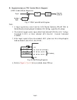
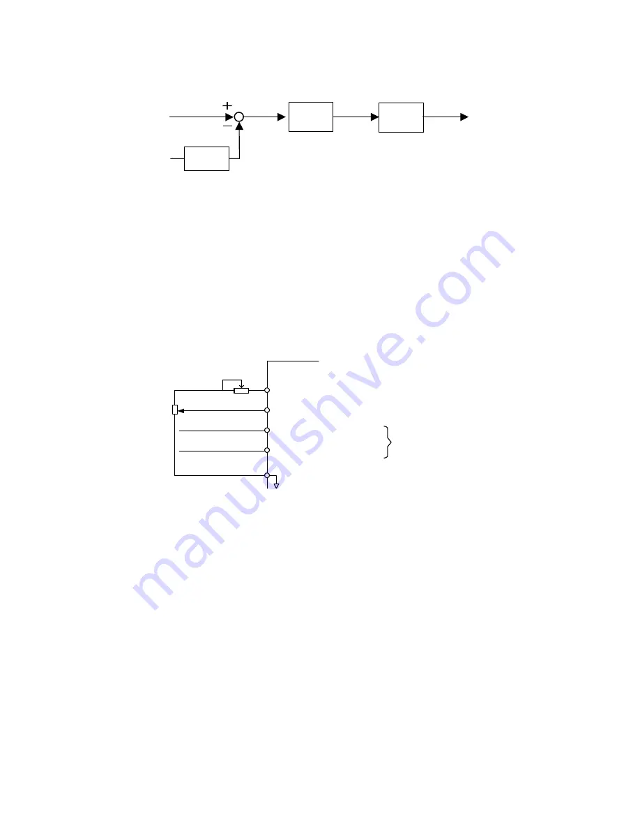
A PID Control Block Diagram is:
Frequency
Command
Primary
Delay
Target
Feedback
Signal
PID
Bn-16
Fig. 47.
PID Control Block Diagram
Note :
1.
A target signal may come from the LCD Digital Operator, RS-485 Port or
Multi-Function Analog Input Terminal-AUX Setting. (upon Sn-05 setting).
2.
The detected signal can be input either from terminal VIN (Sn-24=0, Voltage
Command 0~10V) or from terminal AIN (Sn-24=1, Current Command
4~20mA).
3.
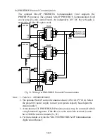
If the target signal is from the terminal AUX, please use the wiring diagram
indicated below: (Sn-05=01, Sn-29=09).
0 ~ +10V
4 ~ 20 mA
0 ~ +10V
GND
+12V
AIN Ref. Com. (Sn-24=1)
VIN Ref. Com. (Sn-24=0)
AUX (Sn-29 = 09 for PID target)
(PID feedback)
Fig. 48.
PID Wiring Diagram
4.
Refer to
Pages 3-7 to 3-9
for more details about PID use.


