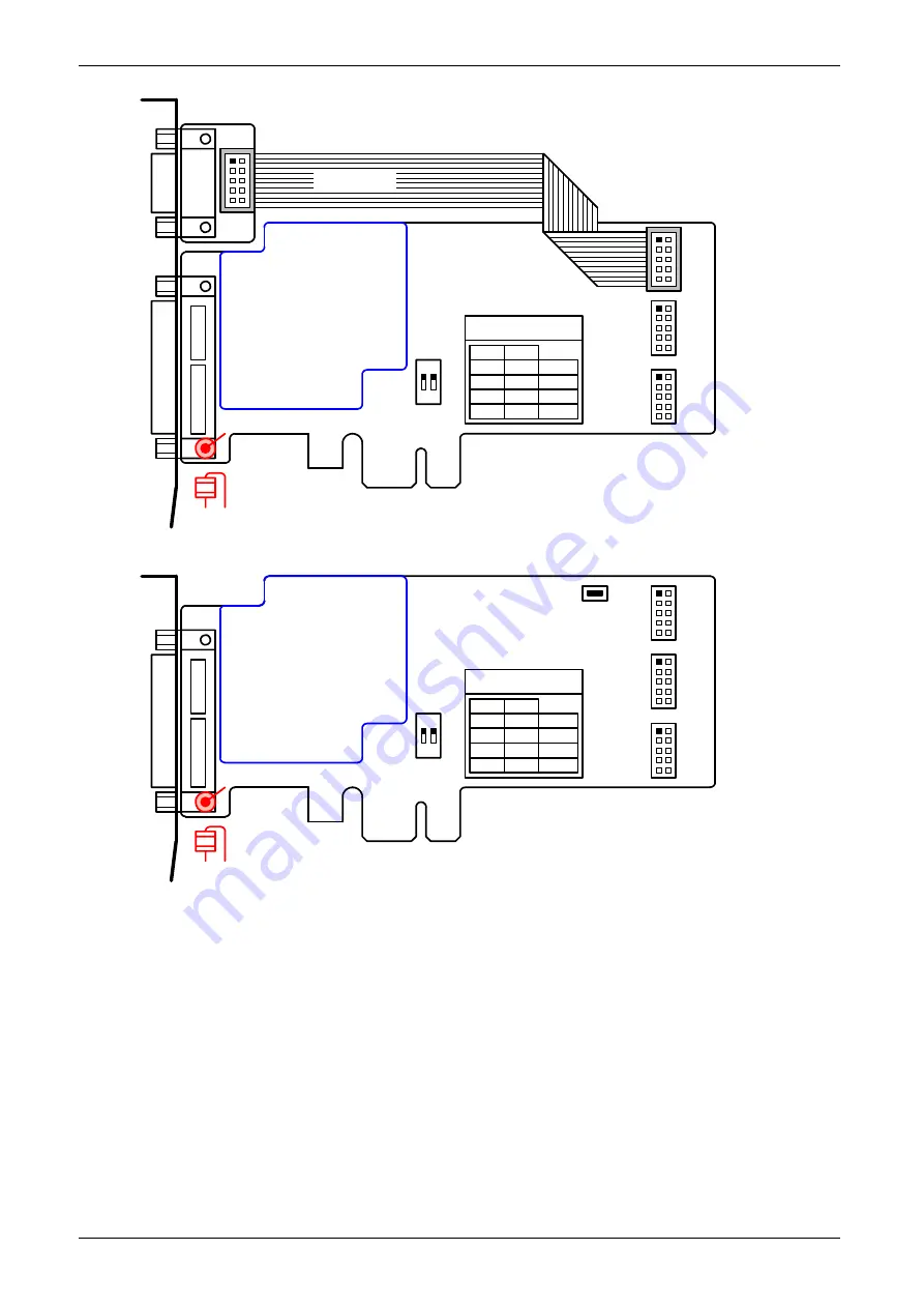
Figure 1.
Location of switches and connectors on both version of cards.
K1
connector of analog inputs and outputs (D-Sub 25 - male)
KX1
connector of digital port DIO0, ie. DIO00÷07 signals (2x5 pin header type)
KX2
connector of digital port DIO1, ie. DIO08÷15 signals (2x5 pin header type)
KX3
connector of digital port DIO2, ie. DIO16÷23 signals (2x5 pin header type)
SW1
DIP switch for identifying multiple cards (CardID value)
PCE-8019
adapter cable PCE-8019 terminated with D-Sub 9 male connector
(included in the delivery package of the standard format card)
KE1
button for activating backup firmware (intended for service purposes)
SA1
Surge Arrester (cards with ESD-X1 option)
PCA-8428, PCA-8429, PCA-8438, PCA-8439
User guide - Appendix, Tables and Figures
rev. 12.2015
II - 1
K1
KX1
SW1
Ser.No.
1 2
ON
ON
ON
ON
OFF
OFF
OFF
OFF
ID=0
S1
S2
ID=1
ID=2
ID=3
KX2
Card ID
KX3
PCE-8019
PCA-84xx
K1
KX1
SW1
Ser.No.
1 2
ON
ON
ON
ON
OFF
OFF
OFF
OFF
ID=0
S1
S2
ID=1
ID=2
ID=3
KX2
PCA-8688
Card ID
KX3
PCA-84xx/LP
SA1
SA1
KE1
ADC16A module
ADC16A module
PCA-8688
(analog IN/OUT)
(analog IN/OUT)
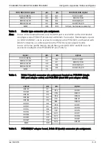
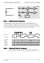
Summary of Contents for PCA-8428
Page 1: ...Multifunctional DAQ PCIe card PCA 8428 8429 8438 8439 User Guide ...
Page 22: ... PCA 8428 PCA 8429 PCA 8438 PCA 8439 User Guide Notes ...
Page 23: ......
Page 24: ......


