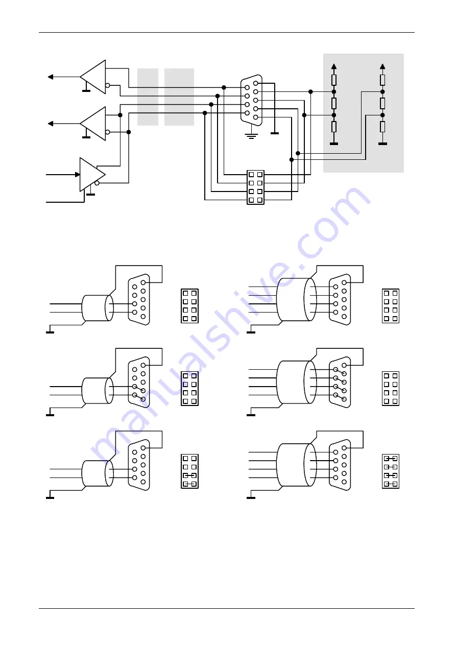
Figure 4. Internal circuit schematics of the RS-422/485 interface using the D-Sub 9
connector.
Figure 5. Schematics of the leading cables connection at RS-485 (a-c) and RS-422 (d-e).
The above figures show the schematics for RS-485 (Figure 5a.),
RS-485 with termination impedances activated by connecting the D-Sub 9 pins (Figure 5b.),
RS-485 with termination impedances activated by jumpers (Figure 5c.), RS-422 (Figure 5d.),
RS-422 with termination impedances activated by connecting the D-Sub 9 pins (Figure 5e.) and
RS-422 with termination impedances activated by jumpers (Figure 5f.).
PCI Express Communication Cards
User guide - Appendix II, Tables and Figures
rev. 10.2009
II - 5
470R
150R
150R
470R
470R
470R
1
2
3
4
5
6
7
8
9
RXD+
RXD-
TXD/RXD+
TXD/RXD-
+5V
+5V
RXD
RXD
TXD
DTR
TXD+
TXD-
( - - - )
( - - - )
RS-422
RS-485
active termination impedances
included at the card
D-Sub 9
2
4
6
8
1
3
5
7
(RS-422)
(RS-485)
JP1/JP2
1
2
3
4
5
6
7
8
9
D-Sub 9
2
4
6
8
1
3
5
7
JP1/JP2
RXD+
RXD-
TXD+
TXD-
TXD/RXD+
TXD/RXD-
GND
1
2
3
4
5
6
7
8
9
D-Sub 9
2
4
6
8
1
3
5
7
JP1/JP2
TXD/RXD+
TXD/RXD-
GND
1
2
3
4
5
6
7
8
9
D-Sub 9
2
4
6
8
1
3
5
7
JP1/JP2
TXD/RXD+
TXD/RXD-
GND
1
2
3
4
5
6
7
8
9
D-Sub 9
2
4
6
8
1
3
5
7
JP1/JP2
GND
RXD+
RXD-
TXD+
TXD-
1
2
3
4
5
6
7
8
9
D-Sub 9
2
4
6
8
1
3
5
7
JP1/JP2
GND
RXD+
RXD-
TXD+
TXD-
1
2
3
4
5
6
7
8
9
D-Sub 9
2
4
6
8
1
3
5
7
JP1/JP2
GND
Obr. 5d.
Obr. 5e.
Obr. 5f.
Obr. 5a.
Obr. 5b.
Obr. 5c.
Summary of Contents for PCI-1482E
Page 1: ...PCI Express Communication Cards User Guide...
Page 18: ...PCI Express Communication Cards User Guide Notes...
Page 19: ......


