background image

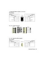
Connector Pinouts  C-3

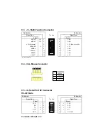
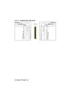
 J4- Serial Port #2 Connector

 (Continued)

RS-485 Mode

Pin Number

Pin Number   

Signal Flow

Top View

Signal Flow

Signal  

   Signal

Reserved

RXD(-)

TXD(-)

Not Connected

GND

-

I/O

O

O

I

1

3

5

7

9

2

4

6

8

10

I

I/O

I

I

-

Not Connected

RXD(+)

TXD(+)

Not Connected

Not Used

C.6 J5 - Power Connector

C.7 J6 - Serial Port #1 Connector

RS-232 Mode

Pin Number

Pin Number   

Signal Flow

Front View

Signal Flow

Signal  

   Signal

CTS

DTR

RI

GND

O
O

I

-

6
7
8
9

1
2
3
4
5

I
I
I

O
O

DCD
DSR
RX
RTS
TX

Summary of Contents for TEK-AT4L Plus

Page 1: ...LE BOARD COMPUTER TECHNICAL REFERENCE MANUAL VERSION 1 1 May 1997 NOTE This manual is for reference purpose only Reproduction in whole or in part is authorized provided TEKNOR INDUSTRIAL COMPUTERS INC...

Page 2: ...the information or use of the products described herein This document may contain or reference information and products protected by the copyrights or patents of others and does not convey any licens...

Page 3: ...G 5 3 5 3 1 Memory Mapping 5 3 5 4 EXPANDED AND EXTENDED MEMORY 5 4 5 4 1 Expanded Memory 5 4 5 4 2 Extended Memory 5 4 5 5 MEMORY MODE 5 4 5 6 SHADOW RAM 5 4 5 7 CONFIGURING THE TEK AT4LPLUS 5 5 5 8...

Page 4: ...7 PARALLEL PRINTER PORT CONNECTOR J7 6 8 6 8 INSTALLING SOLID STATE DISKS 6 9 6 8 1 Writing To Flash Disks 6 9 6 8 2 SRAM Disk 6 9 6 8 3 Battery Backup Circuit 6 10 7 INSTALLING VIDEO DEVICES 7 1 7 1...

Page 5: ...G 5 3 5 3 1 Memory Mapping 5 3 5 4 EXPANDED AND EXTENDED MEMORY 5 4 5 4 1 Expanded Memory 5 4 5 4 2 Extended Memory 5 4 5 5 MEMORY MODE 5 4 5 6 SHADOW RAM 5 4 5 7 CONFIGURING THE TEK AT4LPLUS 5 5 5 8...

Page 6: ...J1 IDE 1 CONNECTOR C 1 C 2 J2 FLOPPY DISK DRIVE CONNECTOR C 1 C 3 J3 MULTI FUNCTION CONNECTOR C 2 C 4 J3A MOUSE CONNECTOR C 2 C 5 J4 SERIAL PORT 2 CONNECTOR C 2 C 6 J5 POWER CONNECTOR C 3 C 7 J6 SERI...

Page 7: ...PRODUCT DESCRIPTION 1 PRODUCT OVERVIEW 2 ONBOARD SUBSYSTEMS...

Page 8: ...s a watchdog timer solid state disks and a power failure detector and can be installed in the most extreme industrial applications CMOS technology makes the TEK AT4LPLUS consume very little power less...

Page 9: ...Product Overview 1 2 TEK AT4LPLUS Block Diagram...

Page 10: ...technology for low power Two years warranty Supports Teknor mezzanine boards The TEK AT4LPLUS single board computer is a versatile board that will function either on a passive backplane or as a stand...

Page 11: ...passive backplane system And when your applications call for it the TEK AT4LPLUS is fully operational without any user interfaces at all able to run without disks keyboard and video 2 4 Diskless Oper...

Page 12: ...INSTALLATION 3 UNPACKING 4 SAFETY PRECAUTIONS 5 CUSTOMIZING THE BOARD 6 INSTALLING DEVICES 7 INSTALLING VIDEO DEVICES 8 SETTING JUMPERS 9 CONFIGURING DMA AND IRQ 10 TEK AT4L PLUS BIOS...

Page 13: ...for possible future shipment F Remove the board from its antistatic wrapping and place it on a grounded surface F Inspect the board for damage If there is any damage or items are missing notify TEKNO...

Page 14: ...a grounding wrist strap before removing the board from its package this will discharge any static electricity that may have built up in your body F Handle the board by the edges 4 2 Storage Environme...

Page 15: ...information 5 2 Installing Memory The TEK AT4LPLUS supports from 1 to 64 Megabytes of DRAM with parity check for system memory The memory must be installed on 30 pin U3 4 5 6 or 72 pin U7 8 SIMM sock...

Page 16: ...kets is near you Hold the module with the notch on the bottom right facing you and insert the connector into the socket at a 70 angle from the board pin 1 on the module lines up with pin 1 on the sock...

Page 17: ...o FFFFFF Flash 600000 67FFFF U36 800000 9FFFFF U19 680000 6FFFFF U28 SRAM A00000 BFFFFF U19 Flash 700000 77FFFF U35 C00000 DF0000 U20 780000 7FFFFF U27 E00000 FFFFFF U20 TABLE 5 2 Onboard Decoded I O...

Page 18: ...e CONFIG SYS file to setup the software in order for it to access memory above 1 MB 5 4 2 Extended Memory In Extended memory mode the CPU s own protected mode is used to access the memory above 1 MB T...

Page 19: ...ystem and what equipment is connected to the system Jumpers WARNING The RAM disk is automatically detected and installed upon booting The beginning of the disk is checked and reformatted if it is foun...

Page 20: ...end of the flat cable Jumper specifies configuration Jumper SW1 1 2 All other drives are installed following the above assignments in this manner RAM Disk and then Hard Disk Therefore with a full conf...

Page 21: ...ollowing parameters 19200 Baud 8 Bits No Parity Echo off or full duplex F Use CTRL R to configure your system in VT100 mode Running Without a Terminal To disconnect the VT100 terminal or to run withou...

Page 22: ...VPP 5v R W bit 3 Enable direction control RS 485 1 enable RS 485 only write only Read PDO Status 4 Make printer 8 data bits read only 1 input 0 output write only 5 Select alternate SW1 SW2 TEK AT4L TE...

Page 23: ...l warning low battery detection W7 2 3 or when monitoring a power supply other than 5VDC W7 1 2 The Power Detection Output PDO of the power failure detection circuit is connected to IOCHECK NMI Jumper...

Page 24: ...rops below 4 75V When this occurs the system is reset disabling access to SRAM DRAM and so on 5 9 4 Low Battery Detection The Low Battery Voltage detection uses the same circuit as the Power Failure D...

Page 25: ...power supply must not be connected together While using one the other must be disconnected 6 1 1 Supplying Power Using the ISA AT Bus 5V 5V 12V 12V and ground voltages are routed on the edge connector...

Page 26: ...Installing Devices 6 3 CONNECTOR LOCATION...

Page 27: ...drive type listed in the setup screen or by using a user defined drive type type 48 whereby the user can enter the required parameters Please refer to your drive manufacturer to obtain this informati...

Page 28: ...and supports Enhanced Floppy Mode 2 88MB It handles 3 5 and 5 25 low and high density drives Up to two drives can be supported in any combination 6 4 PS 2 Mouse Connector J3A The TEK AT4LPLUS support...

Page 29: ...Push button can be connected to reset the TEK733 electrical short between pin 13 and 14 Hard Disk LED the onboard IDE interface drives an external LED during the drive activity Anode must be connected...

Page 30: ...e transceiver J4 3 4 to be controlled by the RTS signal Upon power up or reset the transceiver is by default in receiver mode in order to prevent unwanted perturbation on the line In party line operat...

Page 31: ...0 from the A position leaving the mechanical floppy unused Floppy 0 must then be physically moved to the floppy 1 position where it becomes the B drive Please refer to the Physical Devices Table see...

Page 32: ...no load conditions TEK AT4LPLUS draws approximately 24mA typical This means the battery will last 1 6 years if no power is applied to the board Remember when the 5V is supplied the battery is electron...

Page 33: ...ectly to the Video Adapter onboard connector 7 2 Using Video Mezzanine Board With TEKNOR s mezzanine board it is possible to assembly a complete computer without passive backplane When stand alone mod...

Page 34: ...n W4 DTR2 to DSR2 W19A PS 2 Mouse W5 Serial Out 2 SOUT2 W20 Bus Clock Signal Selection W6 CTS2 W21 CPU Clock Selection W7 1 2 Power Fail Detection W22 Graphic Mode Selection W7 3 4 Low Battery Detecti...

Page 35: ...Setting Jumpers 8 3 JUMPER LOCATIONS...

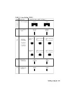
Page 36: ...Setting Jumpers 8 5 TABLE 8 1 Jumper Settings W1 W11...

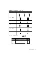
Page 37: ...Setting Jumpers 8 6 TABLE 8 2 Jumper Settings W12 W19 W26...

Page 38: ...Setting Jumpers 8 7 TABLE 8 3 Jumper Settings W20 W25 SW1 SW2...

Page 39: ...Two 8259 interrupt controllers handle the interrupts on the TEK AT4LPLUS Six interrupt lines are directly linked to the keyboard controller timer the real time clock both serial ports and the parallel...

Page 40: ...although the program code itself is different 10 2 ERROR HANDLING Teknor BIOS can be configured to handle errors differently Two possibilities exist Stop The BIOS will stop the booting process if an...

Page 41: ...APPENDICES A PRODUCT SPECIFICATIONS B BOARD DIAGRAMS C CONNECTOR PINOUTS...

Page 42: ...pin connector Serial Ports COM1 RS 232 on a DB9 male connector COM2 RS 232 or RS 485 on a 10 pin connector Parallel Port DB25 male connector Mouse IBM PS 2 mouse compatible 4 pin header Power Supply...

Page 43: ...Board Diagrams B 1 B 1 TEK AT4LPLUS Assembly Diagram Top View...

Page 44: ...Board Diagrams B 3 B 2 TEK AT4LPLUS Mounting Holes...

Page 45: ...Board Diagrams B 5 B 3 TEK AT4LPLUS Mechanical Specifications...

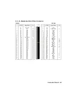
Page 46: ...cted GND GND GND BALE GND IOCS16 Not Connected SA2 CS1 GND Active Low Signal C 2 J2 Floppy Disk Drive Connector Pin Number Pin Number Signal Flow Top View Signal Flow Signal Signal GND GND GND GND GND...

Page 47: ...R KBDINH DOWNL PBRES HDACT I O I O O 1 3 5 7 9 11 13 15 2 4 6 8 10 12 14 16 GND GND VCC Power on LED VCC GND GND GND VCC Active Low Signal C 4 J3A Mouse Connector C 5 J4 Serial Port 2 Connector RS 232...

Page 48: ...Signal Reserved RXD TXD Not Connected GND I O O O I 1 3 5 7 9 2 4 6 8 10 I I O I I Not Connected RXD TXD Not Connected Not Used C 6 J5 Power Connector C 7 J6 Serial Port 1 Connector RS 232 Mode Pin N...

Page 49: ...Number Signal Flow Front View Signal Flow Signal Signal P0 P2 P4 P6 ACK PE AFD INIT GND GND GND GND I O I O I O I O I I O O 2 4 6 8 10 12 14 16 18 20 22 24 1 3 5 7 9 11 13 15 17 19 21 23 25 O I O I O...

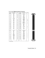
Page 50: ...SA15 SA14 SA13 SA12 SA11 SA10 SA9 SA8 SA7 SA6 SA5 SA4 SA3 SA2 SA1 SA0 I I O I O I O I O I O I O I O I O I O I O I O I O I O I O I O I O I O I O I O I O I O I O I O I O I O I O I O I O I O 2 4 6 8 10...

Page 51: ...22 23 24 25 26 27 28 29 30 31 SBHE LA23 LA22 LA21 LA20 LA19 LA18 LA17 SD08 SD09 SD10 SD11 SD12 SD13 SD14 SD15 MEM CS16 I O CS16 IRQ10 IRQ11 IRQ12 IRQ15 MASTER MEMR MEMW DACK5 DRQ5 DACK6 DRQ6 DACK7 DRQ...

Page 52: ...I O I O I O I O I O I O I O I O I O I O I O I O I O I O I O I O I O I O I O I O I O I O I O I O I O I O I O I O I O I O I O I O I O I O I O I 0 I O I O I O I O I O I O I O C Side B1 B2 B3 B4 B5 B6 B7...

Page 53: ...it suitable for very large scale integration VLSI CMOS are nonvolatile meaning they retain their information even after the power is switched off In a few words CMOS is a digital logic family that is...

Page 54: ...n an industry standard computer any amount of memory above the base configuration supplied by the manufacturer It is the memory above 1 MB accessible only in protected mode Microsoft Windows Xenix and...

Page 55: ...PC AT computer MEMORY MAP A technical reference that shows the entry point and marks the blocks of memory that are reserved for specific functions MEZZANINE CARD MEZZANINE BOARD A peripheral card whi...

Page 56: ...30 times better than that of a magnetic disk SSDs have no moving parts and are less susceptible to dirt moisture vibration and temperature variations than mechanical Floppy disks The Flash EPROM and S...

Page 57: ...DRAM 5 5 E EPROM 5 3 5 5 F Flash Disk 5 6 Flash Disks Writing 6 10 XFLASH 6 10 FLASH EPROM 5 3 Floppy controller 2 1 Full Duplex Operation 6 9 H Hard Disk 5 6 Installation 6 5 Hard Drive Write Precomp...

Page 58: ...tor 2 1 Power Supply 4 1 Power Supply Connector 4 1 R Radioactive 4 1 RAM Disk 5 6 RS 232 5 7 RS 232 or RS 485 2 1 RS 485 6 9 S Safety Precautions 3 1 4 1 Shadow RAM 5 5 Sleep Mode 2 1 Solid State Dis...

Page 59: ...ts or services you may reach us at the above numbers or by writing to LIMITED WARRANTY TEKNOR INDUSTRIAL COMPUTERS INC the seller warrants its products to be free from defects in material and workmans...

Page 60: ...RMA from TEKNOR s Technical Support and clearly mark this number on the outside of the package you are returning To request a number follow these steps make a copy of the request form on the followin...

Page 61: ...Street Address City Province State Country Postal Zip Code Phone Number Fax Number Serial Number Failure or Problem Description P O if not under warranty Fax this form to TEKNOR s Technical Support d...

Reviews: