background image

Onboard Features

7-9

7.7 POWER MANAGEMENT

Power Management features are supported at the BIOS level. All Power Management
options are described in Section 12.3.4 – 

Power Management Setup

.

7.8 SCSI INTERFACE

The board features wide UltraSCSI interface with 32-bit PCI bus master control and zero
wait state transfer capabilities.

The Wide UltraSCSI interface supports operation up to 40Mbytes/sec. Signals are available
through J4 CPCI I/O connector.

SIGNAL PATH

SCSI interface signals are only available through the J4 CPCI I/O connector.

To operate with SCSI devices the onboard SCSI controller must be set by running the
AWARD BIOS setup program (Section 12.3.7 – 

Integrated Peripherals

).

To configure or view the default configuration setting for the SCSI host adapter, use the
Adaptec SCSISelect utility available on the LAN Boot & SCSI Utility diskette 2.

To install the appropriate SCSI driver for a specific operating system, use the EZ-SCSI
software available on the SCSI Utility diskette 1.

Summary of Contents for TEK-CPCI 1003

Page 1: ...only Reproduction in whole or in part is authorized provided TEKNOR INDUSTRIAL COMPUTERS INC is cited as the original source ref M1003_1 1 TEK CPCI 1003 CompactPCI Mobile PENTIUM II SBC TECHNICAL REF...

Page 2: ...4 1 4 1 STATIC ELECTRICITY 4 1 4 2 STORAGE ENVIRONMENT 4 1 4 3 POWER SUPPLY 4 1 5 ONBOARD INTERCONNECTIVITY 5 1 5 1 CONNECTOR LOCATION 5 4 5 2 ONBOARD CONNECTORS AND HEADERS 5 5 5 3 FRONT PLATE CONNEC...

Page 3: ...ENT 7 9 7 8 SCSI INTERFACE 7 9 7 9 SERIAL PORTS 7 10 7 10 THERMAL MANAGEMENT 7 14 7 11 USB INTERFACES 7 15 7 12 VIDEO INTERFACE 7 16 7 13 V PORT 7 18 PART THREE Installation and Settings 8 CUSTOMIZING...

Page 4: ...1 6 PART FOUR Software Setups 12 AWARD SETUP PROGRAM 12 1 12 1 ACCESSING THE AWARD SETUP PROGRAM 12 2 12 2 USING AWARD SETUP PROGRAM 12 3 12 3 SETUPS 12 5 13 UPDATING THE BIOS WITH UPGBIOS 13 1 13 1 C...

Page 5: ...PRODUCT DESCRIPTION 1 PRODUCT OVERVIEW 2 COMPATIBILITY WITH TEKNOR PRODUCTS 3 UNPACKING 4 SAFETY PRECAUTIONS 5 ONBOARD CONNECTIVITY 6 MEZZANINE CONCEPTS...

Page 6: ...el I O interfacing no interconnection capability available on the front plate through CPCI I O connectors The front plate may be adapted optional to support standard mouse keyboard and floppy connecti...

Page 7: ...urst cache is implemented to enhance the processor operations by eliminating wait states on cache accesses CompactPCI Connectors Rear panel CPCI connectors are PICMG 2 0 R2 1 CompactPCI specification...

Page 8: ...ilable on individual local headers A backplane dedicated to the TEK CPCI 1003 is provided by TEKNOR and is referred to as TEK CPCI 1103 CPCI Passive Backplane Mezzanine The mezzanine is a new hardware...

Page 9: ...ystem board TEK CPCI 1103 8 slots CompactPCI backplane TEK CPCI 1106 16 slots CompactPCI backplane TEK CPCI 1050 HD FD keyboard and mouse mezzanine TEK CPCI 1051 HD FD keyboard mouse and PCI to PCI br...

Page 10: ...ure shipment 2 Remove the board from its antistatic wrapping and place it on a grounded surface 3 Inspect the board for damage If there is any damage or items are missing notify TEKNOR immediately Con...

Page 11: ...ing wrist strap before removing the board from its package this will discharge any static electricity that may have built up in your body 3 Handle the board by the edges 4 2 STORAGE ENVIRONMENT Electr...

Page 12: ...e the ISA bus to the Primary PCI bus n Mobile Pentium II processor The TEK CPCI 1003 system board supports 233MHz 266MHz and 300MHz Mobile Pentium II processors from Intel which is the first implement...

Page 13: ...3V 16 Bit ISA Bus Intel 82443BX North Bridge 492PBGA CompactPCI J1 Connector CompactPCI J2 Connector SVGA VPort AGP Termin 3x168P DIMM 3 3V GTL Switching Regulators Clocks Synthes Buffers CPLD Glue Lo...

Page 14: ...lity In addition it supports buffering of simultaneous multiple posted writes and delayed transactions in both directions The PCI to PCI bridge allows the Primary and Secondary PCI buses to operate co...

Page 15: ...TEK CPCI 1003 Technical Reference Manual 5 4 5 1 CONNECTOR LOCATION...

Page 16: ...d to the TEKNOR s CompactFlash module to support CompactFlash disks PCI Mezzanine Connector J14 This connector handles PCI bus signals to the mezzanine DIMM Sockets J16 J17 J18 Three 168 pin DIMM sock...

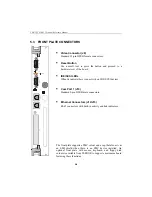
Page 17: ...icate there is an activity on IDE SCSI devices Com Port 1 J10 Standard 9 pin DSUB male connectors Ethernet Connectors J12 J15 RJ 45 connectors with built in activity and link indicators The front plat...

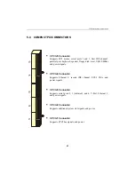
Page 18: ...speaker floppy disk reset USB SMBus and power signals CPCI J4 Connector Supports Ethernet 0 second IDE channel SCSI VGA and power signals CPCI J3 Connector Supports serial ports 2 3 Infrared and 4 V...

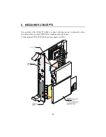
Page 19: ...CONCEPTS The capability of the TEK CPCI 1003 to connect with other devices is enforced by three mezzanine board concepts TEKNOR has implemented on the board A fully equipped TEK CPCI 1003 board may ap...

Page 20: ...is provided by TEKNOR Many other functions will be available soon For more information please contact TEKNOR s offices 6 2 PMC CONCEPT PCI Mezzanine Card PMC is a standard specification that allows PC...

Page 21: ...thod of storing and transferring data It is supported on the board as a standard IDE drive and connects to the EIDE 0 interface The CompactFlash drive can be set as a Master or Slave device and combin...

Page 22: ...FEATURE DESCRIPTION 7 ONBOARD FEATURES...

Page 23: ...ugged typical M T B F is 1 000 000 hours and low power Available capacities are up to 24MB 40 and 80MB modules will be supported when available The C Flash disk connects on the TEK CPCI 1003 via the o...

Page 24: ...nterface It must be declared the same way as a standard hard disk using the BIOS setup program Autodetect Function To setup the CompactFlash disk for Master or Slave configuration use the W5 jumper lo...

Page 25: ...the J19 Mezzanine connector Secondary EIDE interface is only available through the J4 CPCI I O connector The IDE interfaces supports PIO IDE transfers up to 14MB sec and Bus Master IDE transfer up to...

Page 26: ...rdered for the board Front Plate Configuration Ethernet 0 and 1 signals are respectively available on J15 and J12 RJ 45 connectors only when the board is ordered for front plate operations Activity an...

Page 27: ...1 R256 ETX 0 R263 ETX 1 R261 ETX 0 R265 ETX 1 R260 CAUTION Ethernet interfaces are provided factory connected on CPCI I O connectors only when the board is ordered for Rear Panel I O configuration Th...

Page 28: ...When connecting floppy disk drives to the board FD0 and FD1 device combination must be shared in respect of the device allocation capability of the floppy disk interface Two FD0 devices or FD1 device...

Page 29: ...ssignation of the pins on the connector Differences are described as follows Pin Number J5 Standard Mode EPP Mode ECP Mode A15 SLCT SLCT B15 PE PERROR1 ACKREVERS2 C15 BUSY WAIT BUSY1 PERIPHACK2 D15 AC...

Page 30: ...t parallel port devices to share a single parallel port A Daisy Chain device has two ports input and output The input port is connected either to the host parallel port or the daisy chain device in fr...

Page 31: ...Signals are available through J4 CPCI I O connector SIGNAL PATH SCSI interface signals are only available through the J4 CPCI I O connector To operate with SCSI devices the onboard SCSI controller mu...

Page 32: ...ndividually addressable and fully programmable 7 9 1 Serial Port 1 Serial Port 1 is buffered directly for RS 232 operation Signals include the complete signal set for handshaking modem control interru...

Page 33: ...rts Infrared RS 232 RS 422 and RS 485 operation modes When assigned as COM3 the port is 100 compatible with the IBM AT serial port in RS 232 mode RS 422 and RS 485 modes allow communication using diff...

Page 34: ...signals are provided to drive IR module for remote operations through Serial Port 3 When set in IR mode the IR interface supports multi protocol infrared operations The IR interface is IrDA 1 1 compl...

Page 35: ...upon power up or reset the transceiver is by default in receiver mode to prevent unwanted perturbation on the line Party line operation mode requires termination resistors to be installed at both ends...

Page 36: ...ns under the low temperature limit normal condition Thermal management operations are controlled by the BX chipset and settings are provided through the BIOS setup program interface Thermal Management...

Page 37: ...s transfer rate and standardization of peripheral interfaces into a single format SIGNAL PATHS Both USB 0 and USB 1 interface signals are available through the J5 CPCI I O connector USB supports Plug...

Page 38: ...e output configuration you have ordered for the board Front Plate Configuration VGA interface signals are available on J8 standard SVGA video connector located on the front plate of the board only whe...

Page 39: ...olors non interlaced 16 bit images are displayed at up to 1024x768 resolution and 256 color modes can reach a maximum of 1600x1200 resolution Rambus The Rambus interface offers up to 600MB sec bandwid...

Page 40: ...V Port captures video off screen buffers from which it is displayed with resizing and color space conversion Once initiated capture and display occurs with a minimum of processor intervention The I2 C...

Page 41: ...INSTALLATION AND SETTINGS 8 CUSTOMIZING THE BOARD 9 SETTING JUMPERS 10 BUILDING A CPCI SYSTEM 11 CPCI I O SIGNALS...

Page 42: ...tage must be set at the adequate value using the W1 jumper and according to the following table W1 Jumper Setting Processor Core Voltage 1 2 1 2 3 4 5 6 7 8 Vcore MP II 233MHz 1 7V on on on off on 1 6...

Page 43: ...e battery must be connected as follows WARNING Danger of explosion if battery is incorrectly replaced Replace only with the same or equivalent type recommended by the manufacturer Dispose of used batt...

Page 44: ...66MHz SDRAM Serial Presence Detect SPD EEPROM Errors Checking and Correction ECC capabilities or parity bit with 72 bit modules Compliant with Intel s PC SDRAM Unbuffered DIMM Specification 66MHz Rev...

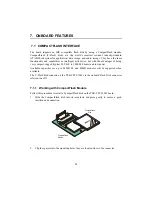
Page 45: ...proceed as follows 1 With the board flat on the table turn it so that the front plate is facing you 2 Hold the module vertically so that the bottom connector key is on the right Insert the fingers in...

Page 46: ...ail output signal goes low The status of the PFO signal can be read at I O address 4031h bit 1 0 failed 1 good The PFO signal can also be connected to the IOCHK signal to generate an NMI non maskable...

Page 47: ...d C248 sets the second stage timeout value to 1 6s CAUTION Modifying the Watchdog timeout period will also modify the value of the Reset period according to the following formula 200ms 47pF x C n Sing...

Page 48: ...g on the I O address selected in BIOS setup and must also include the refresh routine n Watchdog Flags The watchdog status can be read from two bits 5 and 6 of the system register located at the addre...

Page 49: ...utputs when the temperature of the processor or the ambient temperature exceeds a programmable high limit and reset its output when the temperature is under a programmable low limit A special routine...

Page 50: ...d circuitry W5 CompactFlash Setting Use this connector to setup the CompactFlash device in Master or Slave configuration W6 VT100 Mode 5 6 When enabled allows VT100 or ANSI terminal connection Downloa...

Page 51: ...TEK CPCI 1003 Technical Reference Manual 9 2 JUMPER LOCATION...

Page 52: ...Setting Jumpers 9 3 JUMPER SETTINGS Table 1...

Page 53: ...TEK CPCI 1003 Technical Reference Manual 9 4 JUMPER SETTINGS TABLE 2...

Page 54: ...PCI backplane storage module power supply unit and ventilation system The main AC power is drawn to the chassis components through an IEC power plug with a 2 stage filter fuse holder and power switch...

Page 55: ...16 CPCI slot backplane TEK CPCI 1106 is also available from TEKNOR It supports two PCI I O segment one is driven directly by the SBC while the other is managed through a PCI to PCI bridge implemented...

Page 56: ...TEK CPCI 1050 1051 attaches directly to the TEK CPCI 1003 6U form factor storage modules are supported when using the TEK CPCI 1103 backplane 10 1 4 Power Supply 6U power supply modules featuring load...

Page 57: ...e 4 Use the extractor handles to disconnect and extract the board from its enclosure 10 2 1 Connector Keying CompactPCI connector support guide lugs to ensure a correct polarized mating A proper matin...

Page 58: ...2 If there is any mechanical resistance while you insert a module first ensure there is no mechanical obstacle and check for the alignment of all parts 5 To engage the board s connectors into the bac...

Page 59: ...7 A5 C5 E5 B4 D4 A3 C3 E3 V Port pixel data VSDA2 A4 I2C data VP HSYNC C4 Horizontal Synch VP VSYNC D2 Vertical Synch EN CAM E4 Enable camera 11 1 2 Ethernet LEDS Signal Pin Assignation J3 Descriptio...

Page 60: ...E11 Transmit Data JRTS4 A12 Ready To Send JCTS4 B12 Clear To Send JRI4 C12 Ring Indicator JDTR4 E12 Data Terminal Ready 11 1 6 IDE LED Signals Signal Pin Assignation J3 Description EXT SIDEACT B18 Sec...

Page 61: ...a byte is ready or is needed by the Target CD C3 Command Data Indicates Command or message phase when asserted and Data phase when not asserted SSEL D3 SCSI Select The line is driven after a successfu...

Page 62: ...B10 Horizontal sync line VSYNC C10 Vertical sync line RED D10 Analog Red video signal GREEN E10 Analog Green video signal BLUE A11 Analog Blue video signal 11 2 4 Ethernet 0 Interface Signal Pin Assig...

Page 63: ...ommand to the IDE device that it may drive data on SDD lines SIORDY B22 Sec I O Channel Ready In normal mode this input signal is driven directly by the corresponding IDE device IORDY signal SDDACK D2...

Page 64: ...drive data on SDD lines PIORDY B5 Prim I O Channel Ready In normal mode this input signal is driven directly by the corresponding IDE device IORDY signal PDDACK D5 Prim DMA Acknowledge This signal dir...

Page 65: ...data FD HDSEL D10 Head select FD DSKCHG E10 Disk change 11 3 4 Serial Port 2 Signal Pin Assignation J5 Description JDCD2 A11 Data Carrier Detect JRXD2 C11 Receive Data JDSR2 D11 Data Set Ready JTXD2...

Page 66: ...ERR D17 Error at printer STB A19 Strobe signal 11 3 7 Miscellaneous Signals Signal Pin Assignation J5 Description SMBDATA B20 Onboard SMbus data SMBALERT C20 Onboard SMbus Alert CPU overheating SMBCL...

Page 67: ...SOFTWARE SETUPS 12 AWARD SETUP PROGRAM 13 UPDATING THE BIOS WITH UPGBIOS 14 VT100 MODE...

Page 68: ...any operating systems and drivers are installed NOTES Make sure you setup the AWARD software prior to installing your operating system and your drivers For systems that need the BIOS to first attempt...

Page 69: ...g CMOS setup parameters ensure that the W4 battery selection jumper is installed to enable the CMOS battery back up please refer to Section 6 2 To run the AWARD Setup program incorporated in the ROM B...

Page 70: ...values for all the BIOS parameters except Standard CMOS which were displayed when you entered the program In BIOS Features Setup Chipset Features Setup Power Management Setup Thermal Management Setup...

Page 71: ...nfiguration This Setup page sets plug and play and PCI configuration options Integrated Peripherals I O susbsystems that depend on the integrated peripherals controller in your system Load Bios Defaul...

Page 72: ...nged and one wishes to set this option to its original value Loading the BIOS or SETUP defaults will affect all the options in this screen or all parameters if defaults are loaded from the Main Menu a...

Page 73: ...device Only three settings are available for the hard disk type Auto 47 user defined and None Type 1 to 46 are not predefined in the system Use auto detect or enter the parameters for the type in the...

Page 74: ...for the boot device s Options are listed as follows A C SCSI C A SCSI C CDROM A CDROM C A D A SCSI E A SCSI F A SCSI SCSI A C SCSI C A C only LS ZIP C Floppy Disk Access Control R W R W R W Read only...

Page 75: ...adow Dis Dis En Dis CC000 CFFFF Shadow Dis Dis En Dis D0000 D3FFF Shadow Dis Dis En Dis D4000 D7FFF Shadow Dis Dis En Dis D8000 DBFFF Shadow Dis Dis En Dis DC000 DFFFF Shadow Dis Dis En Dis Software t...

Page 76: ...d video card drivers may behave strangely in such a case disable this option 8 Bit I O Recovery Time 3 1 1 2 3 4 5 6 7 8 NA 16 Bit I O Recovery Time 2 1 1 2 3 4 NA The I O recovery mechanism adds bus...

Page 77: ...cs Standards Association VESA Use the software supplied for your video subsystem to select video power management values Blank Screen System only writes blanks to the video buffer Video Off After Stan...

Page 78: ...he IRQ 8 Break Suspend option in this setup screen must be Enabled to use the RTC alarm Date of Month Alarm From 0 to 31 This option appears only if Resume by Alarm is enabled It specifies the date in...

Page 79: ...l Management is enabled CPU Low Temp C T B D T B D T B D CPU Overheat C T B D T B D T B D The CPU will be slowed down when it reaches the selected CPU Overheat C temperature or higher Full speed will...

Page 80: ...ce using the interrupt Legacy ISA Devices compliant with the original PC AT bus specification requiring a specific interrupt such as IRQ4 for serial port 1 PCI ISA PnP Devices compliant with the Plug...

Page 81: ...bus master driver If your hard drive and your system software both support Ultra DMA 33 select Auto to enable BIOS support On Chip Primary Secondary PCI IDE En En En Dis The integrated peripheral cont...

Page 82: ...ow Lo or active high Hi IRRX Mode Select IRMod IRMod IRMode IRRX3 IrDA 1 1 mode only Select operating protocol when in IrDA 1 1 mode VT100 Mode on Serial Port 1 or 2 1 1 1 2 3 4 Selects the serial por...

Page 83: ...ere filename is the name of the 256KB BIOS file containing all BIOS files The BIN extension is used for all BIOS files in a single file VGA_filename is the name of the 64KB file or less containing the...

Page 84: ...e or keyboard functions The devices will be damaged and your board rendered inoperative if you disturb the update process The following message appears on the screen when the BIOS writes to the device...

Page 85: ...ooting Update complete successfully wait for the automatic reboot Rebooting in 5 second s If the update is not successful the following message appears under the Status line ERROR general failure prog...

Page 86: ...teps to set up the VT100 mode 1 Connect a monitor and a keyboard to your board and turn on the power 2 Enter into the CMOS Setup program 3 Select the VT100 mode and the appropriate COM port and save y...

Page 87: ...s to be disconnected you must ensure the control lines are in an active state Failing this the system may hang while waiting for the control lines to become active Wiring the system according to the P...

Page 88: ...14 1 APPENDIX A BOARD SPECIFICATIONS B MEMORY AND I O MAPS C BOARD DIAGRAMS D CONNECTOR PINOUTS E BIOS SETUP ERROR CODES...

Page 89: ...instruction Level 2 512KB internal 64 bit wide pipelined burst 256KB I Os USB Two Universal Serial Bus USB ports Serial Four UART serial port configurable as COM1 4 COM3 is configurable as RS 232 RS...

Page 90: ...EIDE 2 Floppy disk Onboard Expansions PCI Mezzanine Card PMC Proprietary mezzanine CompactFlash BIOS Features Award BIOS in Boot Block Flash Auto configuration extended setup Plug and Play tables Dis...

Page 91: ...2 0A max 12V 0 25A max with 233MHz Mobile Pentium II and 32MB DRAM Power Dissipation 32W max Reliability MTBF MIL HDBK 217F Over 100 000 hours 55 C Designed to meet or exceed UL cUL FCC CFR 47 Part 1...

Page 92: ...unction 00000 9FFFF 0 640 KB DRAM A0000 BFFFF Video DRAM C0000 CBFFF Video BIOS System DRAM LAN BIOS around 30KB if activated address may vary D8000 FFFFF SCSI BIOS 18KB at runtime 2KB if no device ad...

Page 93: ...Interrupt Controller 2 0C0 0DF DMA Controller 2 0F0 0F1 0F8 0FF Math Coprocessor 190 197 290 297 390 397 TEKNOR Control Port 1F0 1F7 3F6 Primary IDE 170 177 376 Secondary IDE 3F0 3F7 370 377 Floppy Di...

Page 94: ...or available 1 All functions marked with an asterisk can be disabled or reconfigured 1 Available lines service on board and external PCI ISA PnP devices or a Legacy ISA device B 4 DMA CHANNELS The TEK...

Page 95: ...C 1 C BOARD DIAGRAMS C 1 ASSEMBLY TOP DIAGRAM...

Page 96: ...O Connector J7 Fan Connector J8 CRT VGA Connector Front panel configuration only J10 Serial Port 1 RS 232 Front panel configuration only J11 CompactFLASH Disk Connector J12 Ethernet 1 Connector Front...

Page 97: ...29 30 31 32 33 34 35 36 37 38 39 40 41 42 43 44 45 46 47 B1 B2 B3 B4 B5 B6 B7 B8 B9 B10 B11 B15 B16 B17 B18 B19 B20 B21 B22 B23 B24 B25 B1 B2 B3 B4 B5 B6 B7 B8 B9 B10 B11 B12 B13 B14 B15 B16 B17 B18 B...

Page 98: ...C AD6 5V AD0 3 3V GNT1 GNT2 REQ4 GND N C GND N C GND N C GND N C GND N C GND REQ5 GND REQ6 GND N C GND N C N C 1 2 3 4 5 6 7 8 9 10 11 15 16 17 18 19 20 21 22 23 24 25 26 27 28 29 30 31 32 33 34 35 3...

Page 99: ...JDCD4 JRTS4 JDCD3 JRTS3 N C N C N C N C PWRBT 1 2 3 4 5 6 7 8 9 10 11 12 13 14 15 16 17 18 19 B1 B2 B3 B4 B5 B6 B7 B8 B9 B10 B11 B12 B13 B14 B15 B16 B17 B18 B19 ZVPCLK VSCL2 5V VP3 GND LINKLED 0 Rese...

Page 100: ...15 D16 D17 D18 D19 VACTI VP VSYNC GND VP4 GND LINKLED 1 Reserved Reserved ERX 1 Reserved JDSR4 5V JDSR3 GND N C N C N C COM2 IRRX N C 1 2 3 4 5 6 7 8 9 10 11 12 13 14 15 16 17 18 19 E1 E2 E3 E4 E5 E6...

Page 101: ...37 38 39 40 41 42 43 44 45 46 47 B1 B2 B3 B4 B5 B6 B7 B8 B9 B10 B11 B15 B16 B17 B18 B19 B20 B21 B22 B23 B24 B25 B1 B2 B3 B4 B5 B6 B7 B8 B9 B10 B11 B12 B13 B14 B15 B16 B17 B18 B19 B20 B21 B22 I2C DATA...

Page 102: ...PDD13 PDD15 PDDACK PDA0 PRI PD1 FD DS1 FD WDATA FD HDSEL JDSR2 5V JDSR1 GND ACK PD3 ERR USBG0 USBD0 GND MDATA 5V 1 2 3 4 5 6 7 8 9 10 11 15 16 17 18 19 20 21 22 23 24 25 26 27 28 29 30 31 32 33 34 35...

Page 103: ...ot Connected GND 1 2 3 4 5 Analog GND Analog GND Analog GND Not Connected GND 6 7 8 9 10 Not Connected Not Connected HSYNC VSYNC Not Connected 11 12 13 14 15 1 1 1 6 11 1 10 15 5 D 6 SERIAL PORT 1 RS...

Page 104: ...5 jumper A1 A0 D0 D1 D2 IOCS16 1 3 5 7 9 11 13 15 17 19 21 23 25 27 29 31 33 35 37 39 1 39 2 40 2 4 6 8 10 12 14 16 18 20 22 24 26 28 30 32 34 36 38 40 GND D3 D4 D5 D6 D7 RPCS1 IOR IOW VCC VCC GND GND...

Page 105: ...AD07 AD09 VI O 5V AD13 C BE1 GND PERR 3 3V TRDY GND AD16 3 3V AD20 AD23 GND C BE3 AD26 5V AD30 GND REQ2 VI O 5V CLK0 5V INTD INTA Reserved 5V AD01 AD04 GND AD08 AD10 GND AD15 SB0 3 3V LOCK GND IRDY 3...

Page 106: ...LK KBDAT VCC KBDF GND GND GND GND FD DS1 FD DRVEN1 FD INDEX FD DSKCHG FD MTR0 FD STEP FD GATE FD WRTPTR FD HSEL VCC VCC MDATA KBCLK GND GND GND GND GND FD DRVEN0 FD MTR1 FD DS0 FDET FD DIR FD WDATA FD...

Page 107: ...EVSEL GND PMC SDONE PAR VCC AD12 AD9 GND AD6 AD4 VCC AD2 AD0 GND 1 3 5 7 9 11 13 15 17 19 21 23 25 27 29 31 33 35 37 39 41 43 45 47 49 51 53 55 57 59 61 63 2 4 6 8 10 12 14 16 18 20 22 24 26 28 30 32...

Page 108: ...onnected Not Connected GND Not Connected GND 1 3 5 7 9 11 13 15 17 19 21 23 25 27 29 31 33 35 37 39 41 43 45 47 49 51 53 55 57 59 61 63 2 4 6 8 10 12 14 16 18 20 22 24 26 28 30 32 34 36 38 40 42 44 46...

Page 109: ...BIOS checksum error 22 Error when getting the boot block flash ID code 33 Error when erasing the boot block flash 44 Error when programming the boot block flash 55 Success of the boot block recovery...

Page 110: ...e A and press Enter If you assumed the system would boot from the hard drive make sure the controller is inserted correctly and all cables are properly attached Also be sure the disk is formatted as a...

Page 111: ...EYBOARD ERROR OR NO KEYBOARD PRESENT Cannot initialize the keyboard Make sure the keyboard is attached correctly and no keys are being pressed during the boot If you are purposely configuring the syst...

Page 112: ...messages when the segment that has caused the problem cannot be isolated PRESS A KEY TO REBOOT This will be displayed at the bottom screen when an error occurs that requires you to reboot Press any ke...

Page 113: ...lt show POST BEh 09 Early Cache Initialization 1 Check for Intel s and or Cyrix CPU 2 Early Cache Initialization when cache is separate from chipset 3 Turn off Gate A20 0A Setup Interrupt Vector Table...

Page 114: ...to find out type of video to use Detect and initialize Video Adapter 12 Init T380 if necessary Boot Block in EMERGENCY Try to init Video Card 0E Test Video Memory 1 If CGA or MONO test video memory 2...

Page 115: ...This POST also Detect Report I O PORTS and also Init Super IO 33 3C Reserved Reserved 3C Setup Enable 3D Initialize Install PS 2 Mouse Detect if mouse is present Initialize mouse Install interrupt vec...

Page 116: ...have a valid CRC If not the Emergency procedure is launched 85 AF Reserved Reserved B0 Spurious If interrupt occurs in protected mode B1 Unclaimed NMI If unmasked NMI occurs display Press F1 to disab...

Page 117: ...D1 Power Management Doze mode Trying to go or in Doze mode D2 Power Management Sleep mode Trying to go or in Sleep mode D3 Power Management Suspend mode Trying to go or in Suspend mode D4 DF Debug Av...

Page 118: ...ROCEDURE To run an EMERGENCY PROCEDURE proceed as follows 1 Remove battery jumper 2 Disable the Power Fail Detection function 3 Connected a 1 44MB floppy drive drive A to the board and insert the EMER...

Page 119: ...and EMERDISK TEK type WDISK then press Enter 5 The program may display one of the following messages Emergency Code transferred The emergency diskette has been successfully created Take the appropria...

Page 120: ...r products or services you may reach us at the above numbers or by writing to TEKNOR INDUSTRIAL COMPUTERS INC 616 Cure Boivin Boisbriand Quebec J7G 2A7 CANADA LIMITED WARRANTY TEKNOR INDUSTRIAL COMPUT...

Page 121: ...merchandise make certain you receive an RMA from TEKNOR s Technical Support and clearly mark this number on the outside of the package you are returning To request a number follow these steps make a...

Page 122: ...AUTORIZATION REQUEST Contact Name Company Name Street Address City Country Phone Number Extension Province State Postal Zip Code Fax Number Fax this form to TEKNOR s Technical Support department in C...

Reviews: