Applications—
7A42
PROBING
ECL CIRCUITS
ECL
circuits
are
commonly
operated
with
a
-5.2
V
and
zero-volt
Vee
and
Vcc
supplies.
For
this
configuration,
a
high
logic
level
becomes
-0.8V
and a
low
logic
level
becomes
-1.7V.
The
output
of an
ECL
gate
is
the
emitter
of
an
NPN
transistor
(emitter
follower
stage)
whose
collector
is
connected
to
ground.
The
output
of
the
gate
must be
pulled down
to
a
negative
supply
with
an
external
resistor to
enable
proper
logic levels
to
exist.
Transmission
lines
are
often
used
to connect gates;
the
pull-down
resistor
can
also
terminate
the
transmission
lines
which
often
connect
gates.
This
termination
is
usually
50,
75,
or
100
ohms
connected
to
a
-2V
supply.
To
probe
ECL,
a
500
Ω
10X
passive
probe
would
be
an
attractive
choice
because
of
its
very
low
input capacitance.
However
this
probe
’
s
resistance,
500
Ω
to
ground,
would
form
a
voltage
divider
with
the
gate's
output
termination
resistor.
Figure
3-9
shows an
ECL
emitter-follower
output
stage being probed a)
by
a
standard
500
Ω
probe,
and
b)
by
the
P6230
Variable
Bias/Offset
Probe.
The
divider
can
shift
the
ECL output signal
levels
with
the
low
level
affected
most.
The
de
operating
point
of
the
gate
output
transistor
is
substantially
altered
when
the
standard
probe
is
part
of
the
circuit,
as
illustrated
in
Figure
3-9.
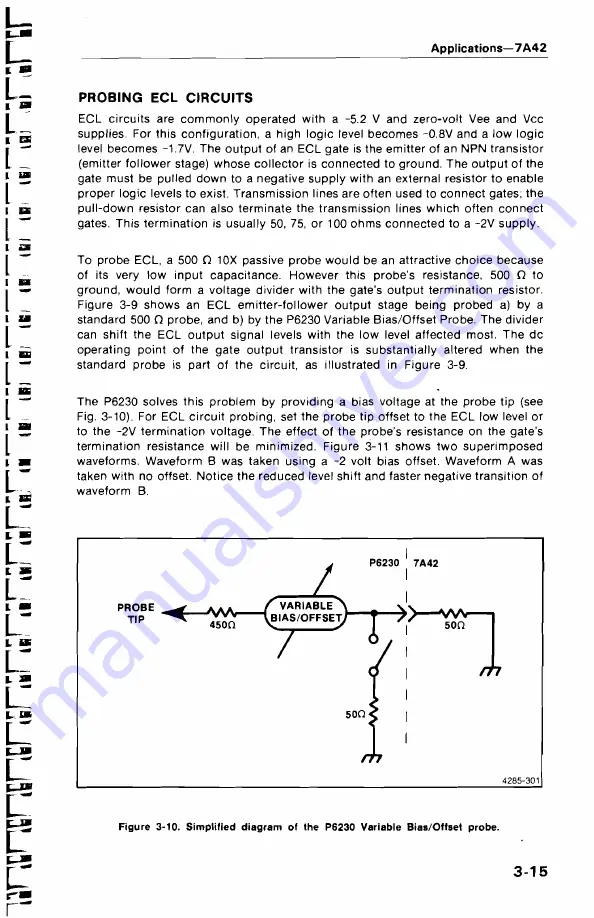
The
P6230
solves
this
problem
by
providing
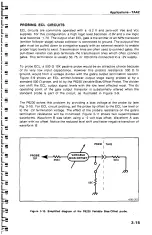
a bias
voltage
at
the
probe
tip (see
Fig.
3-10).
For
ECL
circuit
probing,
set
the
probe
tip offset
to
the
ECL
low
level
or
to
the
-2V
termination
voltage. The
effect
of
the
probe’
s
resistance
on
the
gate's
termination
resistance
will
be
minimized.
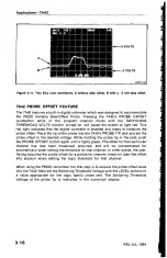
Figure
3-11
shows
two
superimposed
waveforms.
Waveform B
was
taken
using
a
-2
volt
bias
offset.
Waveform
A was
taken
with
no offset. Notice the reduced level
shift
and
faster
negative
transition
of
waveform
B.
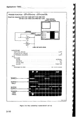
Figure
3-10. Simplified diagram of the P6230 Variable Bias/Offset probe.
3-15


