Maintenance—DM 5010
If these voltages are incorrect,
refer to the Isolated Sup
plies
troubleshooting information. If they are correct, check
the
regulation circuit U1601, U1603, U1605, VR1514,
CR1611, R1611,
and
Q1613 on diagram 2 for the proper
voltages.
Next,
perform one of the troubleshooting
parts, based on
these
symptoms:
part b if the display indicates a 311 error
code;
part c if the displayed measurement is out of specifi
cation
for
the applied
de input voltage.
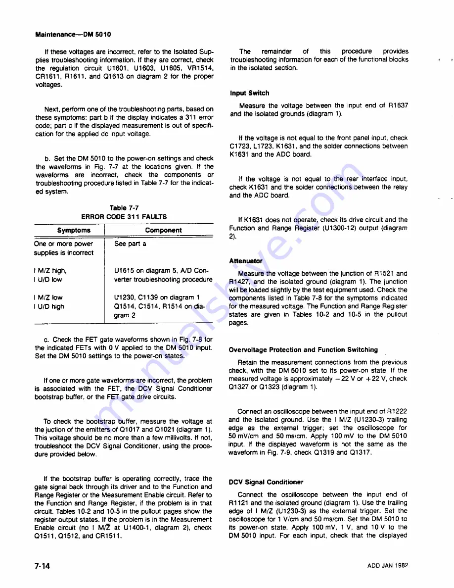
b. Set the DM 5010 to the power-on settings and check
the
waveforms in Fig.
7-7 at the locations given. If the
waveforms
are incorrect, check the components or
troubleshooting procedure
listed in Table 7-7
for the indicat
ed system.
Table
7-7
ERROR CODE
311
FAULTS
Symptoms
Component
One or
more
power
supplies is incorrect
See
part
a
1
M/Z high,
1
U/D
low
U1615
on
diagram
5, A/D Con
verter
troubleshooting
procedure
1
M/Z low
1
U/D
high
U1230,
C1139
on
diagram 1
Q1514,
C1514,
R1514 on dia
gram 2
c.
Check
the FET gate waveforms shown
in Fig. 7-8 for
the
indicated
FETs with 0 V applied to the DM 5010 input.
Set
the DM 5010
settings to the power-on states.
If one or more gate waveforms are incorrect, the
problem
is associated
with the FET,
the DCV Signal
Conditioner
bootstrap buffer, or
the FET gate drive circuits.
To
check
the bootstrap buffer, measure the voltage at
the
juction of the
emitters of Q1
017 and Q1021 (diagram 1).
This
voltage
should be no more than a few millivolts. If not,
troubleshoot
the
DCV Signal Conditioner, using the proce
dure provided below.
If
the
bootstrap buffer is operating correctly, trace the
gate
signal
back through its driver
and to the Function and
Range Register or the Measurement Enable circuit. Refer to
the
Function and
Range Register, if the problem is in that
circuit.
Tables 10-2 and
10-5
in the pullout pages show the
register
output states.
If the problem is
in the Measurement
Enable circuit (no
I M/Z at U1400-1, diagram 2), check
Q1511,
Q1512,
and CR1511.
The
remainder of this procedure provides
troubleshooting
information for each of the functional blocks
in the isolated section.
Input
Switch
Measure
the voltage between the input end of R1637
and the isolated grounds (diagram 1).
If the voltage is not equal to the
front panel input, check
C1723,
L1723, K1631,
and the solder connections between
K1631
and
the
ADC board.
If
the voltage is not equal to the rear interface input,
check K1631
and the solder connections between the relay
and
the
ADC board.
If K1631
does not operate, check its drive circuit and the
Function
and Range Register (U1300-12) output (diagram
2).
Attenuator
Measure
the voltage between the junction of
R1521
and
R1427,
and
the
isolated ground (diagram 1). The junction
will
be loaded slightly by the test equipment used. Check the
components listed in Table 7-8 for the symptoms indicated
for
the measured voltage.
The Function and Range
Register
states
are given
in Tables 10-2 and 10-5 in the pullout
pages.
Overvoltage
Protection and Function Switching
Retain
the measurement connections
from the previous
check,
with the DM 5010 set to its power-on state. If the
measured
voltage is
approximately —22 V or +22 V, check
Q1327
or Q1323 (diagram
1).
Connect
an oscilloscope between the input end of R1222
and
the
isolated ground. Use the I M/Z (U1230-3) trailing
edge
as
the external trigger; set the oscilloscope for
50 mV/cm and 50
ms/cm. Apply 100
mV to
the DM 5010
input. If
the displayed waveform is not the same as the
waveform
in Fig. 7-9, check Q1319 and Q1317.
DCV
Signal Conditioner
Connect
the
oscilloscope between the input end of
R1121
and the isolated ground (diagram 1). Use the trailing
edge
of I
M/Z (U1230-3) as the
external trigger. Set the
oscilloscope for 1
V/cm and 50 ms/cm. Set the DM 5010 to
its
power-on state. Apply 100 mV, 1
V, and 10 V to the
DM5010 input.
For
each input, check that the displayed
7-14
ADD
JAN
1982
Summary of Contents for DM 5010
Page 14: ...DM 5010 2994 00 DM 5010 Programmable Digital Multimeter xii ADD JUL 1986...
Page 27: ...Operating Instructions DM 5010 2994 03 Fig 2 3 DM 5010 front panel controls and connectors 2 3...
Page 38: ......
Page 134: ......
Page 208: ......
Page 222: ......
Page 250: ......
Page 251: ...Section 8 DM 5010 OPTIONS No options are available 8 1...
Page 252: ......
Page 270: ......
Page 272: ...DM 5010 2994 37 Fig 10 2 Location of DM 5010 adjustments and test points...
Page 273: ......
Page 274: ......
Page 275: ......
Page 276: ...DM 5010 2994 112 DM 5010 BLOCK DIAGRAM...
Page 281: ......
Page 282: ......
Page 291: ......
Page 293: ......
Page 294: ......
Page 297: ......
Page 298: ......
Page 303: ......
Page 304: ...I...
Page 305: ......
Page 310: ......
Page 311: ......
Page 315: ......
Page 318: ......
Page 321: ......
Page 323: ......
Page 326: ......
Page 332: ...2994 57...
Page 334: ......
Page 335: ......
Page 336: ......
Page 337: ...63 REV JUN 1986...
Page 338: ...FIG 1 EXPLODED DM 5010...
Page 339: ......
Page 340: ......
Page 341: ......
Page 347: ......


