background image

Performance Verification

4–34

SPG 422 Service Manual (B034000 and above)

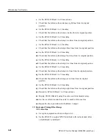
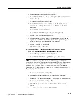
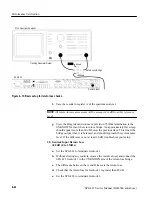
g. Check, using the 1780 waveform monitor, that the genlock input signal

has a signal to noise ratio better than 50 dB. (If this signal is not good
enough, you will need to find another signal source.)

h. Display CH B1 on the 1780 vectorscope.

i.

Check for less than 0.5

°

 of jitter.

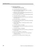
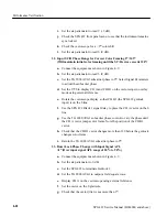
29. Pull-in Range

Subcarrier Frequency 

±

20 Hz

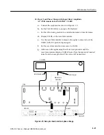
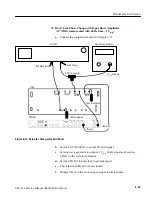
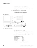
a. Connect the equipment as shown in Figure 4–9.

b. Set the SPG 422 to burst lock, genlock loopthrough but do not terminate

the loopthrough.

c.

Set the Step Attenuator to 6 dB (actually 0 dB of attenuation).

d. Set the TG 2000 BG1 and AVG1 modules to NTSC. You must set each

generator.

e.

Set the TG 2000 AVG1 module to output a 0% flat field.

f.

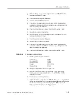
Set the TG 2000 AVG1 to provide 20 Hz of subcarrier variation. Select
the Active Signal Parameters and select the Subcarrier to adjust it. See
the TG 2000/AVG1 manual for detailed instructions to make these
settings.

g. Set the 1780 to display CH A and CH B1 in parade format using

external reference.

h. Set the SPG 422 Genlock to loopthrough.

i.

Set the SPG 422 Black 1 to output a NTSC black burst signal with no
delay.

j.

Check that the SPG 422 is genlocked (front-panel External Ref LED is
lit).

k. Set the TG 2000 AVG1 to output the 0% flat field signal with –20 Hz

subcarrier variation.

l.

Check that the SPG 422 remains genlocked.

m. Set the TG 2000 AVG1 to output the 0% flat field signal with +20 Hz

subcarrier variation.

n. Check that the SPG 422 remains genlocked.

o. Return the TG 2000 AVG1 to a normal subcarrier signal.

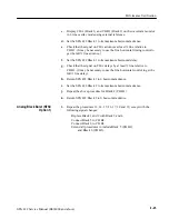
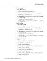
30. Sync Lock Jitter

 0.6 nsec (0.75

°

 at 3.58 MHz, 1

°

 at 4.43 MHz, SNR >50 dB)

Summary of Contents for SPG 422

Page 1: ...r S N B034000 and above 071 0596 00 Warning The servicing instructions are for use by qualified personnel only To avoid personal injury do not perform any servicing unless you are qualified to do so Refer to all safety summaries prior to performing service ...

Page 2: ...atents issued and pending Information in this publication supercedes that in all previously published material Specifications and price change privileges reserved Printed in the U S A Tektronix Inc P O Box 1000 Wilsonville OR 97070 1000 TEKTRONIX and TEK are registered trademarks of Tektronix Inc ...

Page 3: ...ations This warranty shall not apply to any defect failure or damage caused by improper use or improper or inadequate maintenance and care Tektronix shall not be obligated to furnish service under this warranty a to repair damage resulting from attempts by personnel other than Tektronix representatives to install repair or service the product b to repair damage resulting from improper use or conne...

Page 4: ......

Page 5: ...g 2 2 Black Signals 2 3 Bars Signals 2 3 Serial Black 2 3 Audio Signals 2 4 Serial Signals Option 2 only 2 4 Theory of Operation Genlock 3 1 Front Panel Board 3 1 Digital Board 3 3 Output Board 3 4 Power Supply 3 6 Option 1 Board 3 6 Option 2 Board 3 7 Detailed Circuit Descriptions 3 7 Output Board 3 10 Power Supply 3 15 Option 1 Board 3 21 Option 2 Board 3 23 Performance Verification Equipment Re...

Page 6: ...nspection and Cleaning 6 2 Corrective Maintenance 6 5 Tektronix Service Offerings 6 6 Repackaging Instructions 6 13 Options Power Cord Options 7 1 Ordering 7 2 Replaceable Electrical Parts Parts Ordering Information 8 1 Using the Replaceable Electrical Parts List 8 1 Diagrams Replaceable Mechanical Parts Parts Ordering Information 10 1 Using the Replaceable Mechanical Parts List 10 1 ...

Page 7: ...ure 1 10 75 Color bars CR channel 1 25 Figure 1 11 100 Color bars Y channel 1 25 Figure 1 12 100 Color bars CB channel 1 26 Figure 1 13 100 Color bars CR channel 1 26 Figure 1 14 100 Red Y channel 1 27 Figure 1 15 100 Red CB channel 1 27 Figure 1 16 100 Red CR channel 1 28 Figure 1 17 EIA bars part of SMPTE bars Y channel 1 28 Figure 1 18 EIA bars part of SMPTE bars CB channel 1 29 Figure 1 19 EIA...

Page 8: ...re 1 42 Bowtie CB and CR channels 1 41 Figure 1 43 Bowtie markers Y channel 1 41 Figure 1 44 Ramp Y channel 1 42 Figure 1 45 Ramp CB channel 1 42 Figure 1 46 Ramp CR channel 1 43 Figure 1 47 Pluge Y channel 1 43 Figure 1 48 Pluge CB and CR channels 1 44 Figure 2 1 SPG 422 front panel 2 1 Figure 2 2 Various ways genlock input can be configured 2 2 Figure 2 3 Illustration of SPG 422 timing 2 4 Figur...

Page 9: ...to check the oscillator frequency 4 32 Figure 4 9 Setup to check some genlock functions 4 33 Figure 4 10 Setup to check burst lock phase change 4 37 Figure 4 11 Setup to check genlock with hum 4 39 Figure 4 12 Setup to check isolation 4 40 Figure 4 13 Basic setup for return loss checks 4 42 Figure 5 1 Setup for sync tip adjustment 5 4 ...

Page 10: ...digital audio outputs XLR connectors 1 14 Table 1 9 Signal characteristics for AES EBU serial digital audio outputs BNC outputs 1 14 Table 1 10 Signal characteristics for embedded serial audio 1 15 Table 1 11 20 bit audio signal sample distribution for embedded serial audio on 525 59 94 signals 1 16 Table 1 12 20 bit audio signal sample distribution for embedded serial audio on 625 50 signals 1 16...

Page 11: ...duct ensure that the product is properly grounded Observe All Terminal Ratings To avoid fire or shock hazard observe all ratings and markings on the product Consult the product manual for further ratings information before making connections to the product The common terminal is at ground potential Do not connect the common terminal to elevated voltages Replace Batteries Properly Replace batteries...

Page 12: ...tices that could result in injury or loss of life CAUTION Caution statements identify conditions or practices that could result in damage to this product or other property Terms on the Product These terms may appear on the product DANGER indicates an injury hazard immediately accessible as you read the marking WARNING indicates an injury hazard not immediately accessible as you read the marking CA...

Page 13: ...retain hazardous voltages for long periods of time after power is turned off Before attempting any servicing discharge the CRT by shorting the anode to chassis ground When discharging the CRT connect the discharge path to ground and then the anode Rough handling may cause the CRT to implode Do not nick or scratch the glass or subject it to undue pressure when removing or installing it When handlin...

Page 14: ...Service Safety Summary x SPG 422 Service Manual B034000 and above ...

Page 15: ...f Operation provides a block diagram description of the instrument circuits H Performance Verification provides a manual procedure for verifying the performance requirements in the Specifications section H Adjustment Procedures provides an automated procedure for adjusting the generator following repair H Maintenance provides instructions for troubleshooting and replacing instrument modules H Opti...

Page 16: ...ntact us by e mail tm_app_supp tektronix com For product support outside of North America contact your local Tektronix distributor or sales office Service Support Contact your local Tektronix distributor or sales office Or visit our web site for a listing of worldwide service locations www tektronix com For other information In North America 1 800 TEK WIDE 1 800 835 9433 An operator will direct yo...

Page 17: ......

Page 18: ...m an AC power source that will not apply more than 250 VRMS between the supply conductors or either supply conductor and ground A protective ground connection by way of the grounding conductor is essential for safe operation Environmental specifications are listed toward the back of the following tables In addition a list of appropriate safety and electromagnetic interference EMI standards also ca...

Page 19: ...U Tech 3267 E Coded Signals Luminance Y and color difference Cr and Cb Number of Samples per Video Line 525 59 94 625 50 Luminance Y 858 864 Color Difference Cr and Cb 429 432 Sampling Structure Orthogonal line field and frame repetitive Cr and Cb samples are co sited with odd Y samples in each line Sampling Frequency Luminance Y 13 5 MHz nominal Color Difference Cr and Cb 6 75 MHz nominal Signal ...

Page 20: ...5 50 See Figure 1 3 525 59 94 See Figure 1 4 Timing Reference Signal Bit 1st Word 2nd Word 3rd Word 4th Word End of Active Video Start o Active i eo A A 9 1 0 0 1 of Active Video EAV SAV 8 1 0 0 F 7 1 0 0 V 6 1 0 0 H 5 1 0 0 P3 4 1 0 0 P2 3 1 0 0 P1 2 1 0 0 P0 1 1 0 0 0 0 1 0 0 0 where F 1 during field 2 V 1 during vertical blanking H 1 during horizontal blanking The protection bits are F V H P3 P...

Page 21: ... 1 Timing relationship between digital video data and analog line synchronization reference for line scanning in the 525 60 system Totale line 1728 words Digital active line 1440 words 0 1439 Digital H interval 288 words 1440 1727 EVA 4 words SAV 4 words Analog line EVA 4 words Figure 1 2 Timing relationship between digital video data and analog line synchronization reference for line scanning in ...

Page 22: ...pecifications SPG 422 Service Manual B034000 and above 1 5 623 Figure 1 3 Relationship between digital and analog fields showing also the position of the digital field blanking interval in the 625 system ...

Page 23: ...Specifications 1 6 SPG 422 Service Manual B034000 and above Figure 1 4 Relationship of video data vertical sync in 525 system ...

Page 24: ...red between 20 and 80 amplitude points Difference Between Rise and Fall Time 0 5 nsec Measured between 20 and 80 amplitude points Jitter Less than 0 25 nsec over a period of one video line Required Receiver Termination 75 W with return loss 15 dB from 5 MHz to 270 MHz Table 1 4 Signal characteristics for analog black outputs base instrument only Characteristics Performance requirements Supplementa...

Page 25: ...subcarrier Burst Duration NTSC 9 cycles of subcarrier PAL 10 cycles of subcarrier Burst Frequency NTSC 3 579545 MHz 1 Hz PAL 4 43361875 MHz 1 Hz SC H Phase Accuracy 0 5 Field Timing Offset Range 2 fields Relative to the genlock input Field Timing Offset Resolution Video field increments Vertical Timing Offset Range 8 lines Relative to the genlock input Vertical Timing Offset Resolution Video line ...

Page 26: ...RE PAL 300 mV 15 mV White Flag Level PAL only 0 or 700 mV user selectable Sync Timing NTSC See Figures 1 5 and 1 6 PAL See Figure 1 7 Burst Rise Time NTSC 400 nsec PAL 350 nsec Burst Amplitude NTSC 40 IREp p 2 IRE PAL 300 mVp p 15 mV Burst Delay from Sync NTSC 19 cycles of subcarrier PAL 25 cycles of subcarrier Burst Duration NTSC 9 cycles of subcarrier PAL 10 cycles of subcarrier Burst Frequency ...

Page 27: ...ption 1 only cont Characteristics Supplemental information Performance requirements Vertical Timing Offset Resolution Video line increments Horizontal Timing Offset Range 1 2 video line Horizontal Timing Offset Resolution Single 27 MHz clock cycles Return Loss 30 dB 0 5 MHz Figure 1 5 60 Hz black burst with 7 5 IRE setup ...

Page 28: ...Specifications SPG 422 Service Manual B034000 and above 1 11 Figure 1 6 60 Hz black burst with no setup Figure 1 7 50 Hz black burst ...

Page 29: ...7 310 100 Bars over Red Field Timing Color Bars Red 625 50 format only See Figures 1 11 1 12 1 13 1 14 1 15 and 1 16 Lines 23 166 Lines 167 310 100 Full Field Bars 525 and 625 formats available See Figures 1 11 1 12 and 1 13 Serial Black 525 and 625 formats available Error Detection and Handling Insertion Can be enabled or disabled by user Field Timing Offset Range 1 field Relative to the genlock ...

Page 30: ... and 1 27 Pulse And Bar See Figures 1 29 and 1 31 Ramp See Figures 1 44 1 45 and 1 46 Serial Digital Interface SDI matrix Matrix consists of Bit Slip and Clock Recovery Test signal and the Equalizer signal per SMPTE RP 178 Bit Slip stresses the recovery ability of the receiver clock regenerator by sending a string of twenty 0s followed by a single 1 The Equalizer Test signal contains a maximum low...

Page 31: ...e emphasis None Jitter on Data transitions Within 20 nsec from an ideal clock Channel Status Bits Uses default settings except explicit data resolution status Emphasis bits may be set to test receivers but do not enable emphasis in the data See Table 4 15 Table 1 9 Signal characteristics for AES EBU serial digital audio outputs BNC outputs Characteristics Performance requirements Supplemental info...

Page 32: ...ÁÁÁÁÁÁÁÁÁÁÁ ÁÁÁÁÁÁÁÁÁÁÁÁ Uses default settings except explicit data resolution status Emphasis bits may be set to test receivers but do not enable empha sis in the data See Table 4 15 Table 1 10 Signal characteristics for embedded serial audio Characteristics Performance requirements Supplemental information ÁÁÁÁÁÁÁÁÁÁÁÁ ÁÁÁÁÁÁÁÁÁÁÁÁ ÁÁÁÁÁÁÁÁÁÁÁÁ Standards Conformance ÁÁÁÁÁÁÁÁÁÁÁÁ ÁÁÁÁÁÁÁÁÁÁÁÁ ÁÁÁ...

Page 33: ...Á ÁÁÁÁÁÁÁÁÁÁ 376 113 ÁÁÁÁÁÁÁÁ ÁÁÁÁÁÁÁÁ 4 ÁÁÁÁÁÁÁÁÁ ÁÁÁÁÁÁÁÁÁ 125 ÁÁÁÁÁÁÁÁÁ ÁÁÁÁÁÁÁÁÁ 4 ÁÁÁÁÁÁÁÁÁÁ ÁÁÁÁÁÁÁÁÁÁ 388 125 ÁÁÁÁÁÁÁÁ ÁÁÁÁÁÁÁÁ 4 ÁÁÁÁÁÁÁÁÁ ÁÁÁÁÁÁÁÁÁ 137 ÁÁÁÁÁÁÁÁÁ ÁÁÁÁÁÁÁÁÁ 4 ÁÁÁÁÁÁÁÁÁÁ ÁÁÁÁÁÁÁÁÁÁ 400 137 ÁÁÁÁÁÁÁÁ ÁÁÁÁÁÁÁÁ 4 ÁÁÁÁÁÁÁÁÁ ÁÁÁÁÁÁÁÁÁ 149 ÁÁÁÁÁÁÁÁÁ ÁÁÁÁÁÁÁÁÁ 4 ÁÁÁÁÁÁÁÁÁÁ ÁÁÁÁÁÁÁÁÁÁ 412 149 ÁÁÁÁÁÁÁÁ ÁÁÁÁÁÁÁÁ 4 ÁÁÁÁÁÁÁÁÁ ÁÁÁÁÁÁÁÁÁ 161 ÁÁÁÁÁÁÁÁÁ ÁÁÁÁÁÁÁÁÁ 4 ÁÁÁÁÁÁÁÁÁÁ ÁÁÁÁÁÁÁÁÁÁ 424...

Page 34: ...ÁÁÁÁ ÁÁÁÁÁÁÁÁ 4 ÁÁÁÁÁÁÁÁÁÁ ÁÁÁÁÁÁÁÁÁÁ 145 ÁÁÁÁÁÁÁÁÁ ÁÁÁÁÁÁÁÁÁ 4 ÁÁÁÁÁÁÁÁÁÁ ÁÁÁÁÁÁÁÁÁÁ 458 145 ÁÁÁÁÁÁÁÁ ÁÁÁÁÁÁÁÁ 4 ÁÁÁÁÁÁÁÁÁÁ ÁÁÁÁÁÁÁÁÁÁ 155 ÁÁÁÁÁÁÁÁÁ ÁÁÁÁÁÁÁÁÁ 4 ÁÁÁÁÁÁÁÁÁÁ ÁÁÁÁÁÁÁÁÁÁ 468 155 ÁÁÁÁÁÁÁÁ ÁÁÁÁÁÁÁÁ 4 ÁÁÁÁÁÁÁÁÁÁ ÁÁÁÁÁÁÁÁÁÁ 165 ÁÁÁÁÁÁÁÁÁ ÁÁÁÁÁÁÁÁÁ 4 ÁÁÁÁÁÁÁÁÁÁ ÁÁÁÁÁÁÁÁÁÁ 478 165 ÁÁÁÁÁÁÁÁ ÁÁÁÁÁÁÁÁ 4 ÁÁÁÁÁÁÁÁÁÁ ÁÁÁÁÁÁÁÁÁÁ 175 ÁÁÁÁÁÁÁÁÁ ÁÁÁÁÁÁÁÁÁ 4 ÁÁÁÁÁÁÁÁÁÁ ÁÁÁÁÁÁÁÁÁÁ 488 175 ÁÁÁÁÁÁÁÁ ÁÁÁ...

Page 35: ...ÁÁÁÁÁÁÁÁÁÁÁ Alphanumeric Channel Origin ÁÁÁ ÁÁÁ 8 ÁÁÁÁ ÁÁÁÁ 0 7 ÁÁÁÁÁÁ ÁÁÁÁÁÁ 0000 0001 ÁÁÁÁÁÁÁÁÁÁÁÁÁÁÁÁÁÁÁÁÁÁÁ ÁÁÁÁÁÁÁÁÁÁÁÁÁÁÁÁÁÁÁÁÁÁÁ Alphanumeric Channel Origin ÁÁÁ ÁÁÁ 9 ÁÁÁÁ ÁÁÁÁ 0 7 ÁÁÁÁÁÁ ÁÁÁÁÁÁ 0000 0001 ÁÁÁÁÁÁÁÁÁÁÁÁÁÁÁÁÁÁÁÁÁÁÁ ÁÁÁÁÁÁÁÁÁÁÁÁÁÁÁÁÁÁÁÁÁÁÁ Alphanumeric Channel Origin ÁÁÁ ÁÁÁ 10 ÁÁÁÁ ÁÁÁÁ 0 7 ÁÁÁÁÁÁ ÁÁÁÁÁÁ 0000 0001 ÁÁÁÁÁÁÁÁÁÁÁÁÁÁÁÁÁÁÁÁÁÁÁ ÁÁÁÁÁÁÁÁÁÁÁÁÁÁÁÁÁÁÁÁÁÁÁ Alphanumeric Ch...

Page 36: ...ÁÁÁÁ Burst Lock Jitter ÁÁÁÁÁÁÁÁÁÁÁÁ ÁÁÁÁÁÁÁÁÁÁÁÁ 0 5 ÁÁÁÁÁÁÁÁÁÁÁÁ ÁÁÁÁÁÁÁÁÁÁÁÁ SNR2 50 dB ÁÁÁÁÁÁÁÁÁÁÁÁ ÁÁÁÁÁÁÁÁÁÁÁÁ ÁÁÁÁÁÁÁÁÁÁÁÁ Genlock Noise Performance ÁÁÁÁÁÁÁÁÁÁÁÁ ÁÁÁÁÁÁÁÁÁÁÁÁ ÁÁÁÁÁÁÁÁÁÁÁÁ ÁÁÁÁÁÁÁÁÁÁÁÁ ÁÁÁÁÁÁÁÁÁÁÁÁ ÁÁÁÁÁÁÁÁÁÁÁÁ Will remain locked with SNR 30 dB or 60 Hz hum 1 Vp p ÁÁÁÁÁÁÁÁÁÁÁÁ ÁÁÁÁÁÁÁÁÁÁÁÁ ÁÁÁÁÁÁÁÁÁÁÁÁ Burst Lock Phase Change with Input Burst Amplitude ÁÁÁÁÁÁÁÁÁÁÁÁ ÁÁÁÁÁÁÁÁÁÁ...

Page 37: ...mit 12 V Total power limited to 120 W 5 V 5 V 12 V Hum Typical values 12 V 10 mV 5 V 10 mV 5 V 20 mV 12 V 10 mV Noise 5 MHz measurement bandwidth 12 V 50 mV 5 V 50 mV 5 V 50 mV 12 V 50 mV Line Voltage Range 85 132 VAC 180 250 VAC Supply set for 110 V operation Supply set for 220 V operation Crest Factor 1 35 Fuse Required 2 A med blow 110 V operation 1 A med blow 220 V operation Power Consumption ...

Page 38: ...nce to 40 C Altitude Non operating To 50 000 feet Operating To 15 000 feet 4572 Meters IEC 1010 1 compliance to 2000 Meters Humidity 5 95 humidity non condensing Vibration Operating From 5 to 350 Hz 0 0002 g2 Hz Acceleration Power Spectral Density APSD From 350 to 500 Hz 3 dB Octave Slope At 500 Hz 0 00014 g2 Hz APSD 0 31 GRMS Overall 10 Minutes Axis Non operating From 5 to 100 Hz 0 020 g2 Hz APSD...

Page 39: ... in the Official Journal of the European Communities EN 50081 1 Emissions EN 55022 Class B Radiated and Conducted Emissions EN 60555 2 AC Power Line Harmonic Emissions EN 50082 1 Immunity IEC 801 2 Electrostatic Discharge Immunity IEC 801 3 RF Electromagnetic Field Immunity IEC 801 4 Electrical Fast Transient Burst Immunity IEC 801 5 Power Line Surge Immunity 1 High quality shielded cables must be...

Page 40: ...on Category Descriptions Terminals on this product may have different installation category designations The installation categories are CAT III Distribution level mains usually permanently connected Equipment at this level is typically in a fixed industrial location CAT II Local level mains wall sockets Equipment at this level includes appliances portable tools and similar products Equipment is u...

Page 41: ...Specifications 1 24 SPG 422 Service Manual B034000 and above Signal Illustrations Figure 1 8 75 Color bars Y channel Figure 1 9 75 Color bars CB channel ...

Page 42: ...Specifications SPG 422 Service Manual B034000 and above 1 25 Figure 1 10 75 Color bars CR channel Figure 1 11 100 Color bars Y channel ...

Page 43: ...Specifications 1 26 SPG 422 Service Manual B034000 and above Figure 1 12 100 Color bars CB channel Figure 1 13 100 Color bars CR channel ...

Page 44: ...Specifications SPG 422 Service Manual B034000 and above 1 27 Figure 1 14 100 Red Y channel Figure 1 15 100 Red CB channel ...

Page 45: ...Specifications 1 28 SPG 422 Service Manual B034000 and above Figure 1 16 100 Red CR channel Figure 1 17 EIA bars part of SMPTE bars Y channel ...

Page 46: ...Specifications SPG 422 Service Manual B034000 and above 1 29 Figure 1 18 EIA bars part of SMPTE bars CB channel Figure 1 19 EIA bars part of SMPTE bars CR channel ...

Page 47: ...Specifications 1 30 SPG 422 Service Manual B034000 and above Figure 1 20 IWQ bars part of SMPTE bars Y channel Figure 1 21 IWQ bars part of SMPTE bars CB channel ...

Page 48: ...Specifications SPG 422 Service Manual B034000 and above 1 31 Figure 1 22 IWQ bars part of SMPTE bars CR channel Figure 1 23 Reverse bars part of SMPTE bars Y channel ...

Page 49: ...Specifications 1 32 SPG 422 Service Manual B034000 and above Figure 1 24 Reverse bars part of SMPTE bars CB channel Figure 1 25 Reverse bars part of SMPTE bars CR channel ...

Page 50: ...Specifications SPG 422 Service Manual B034000 and above 1 33 Figure 1 26 Multiburst Y channel Figure 1 27 Multiburst for CB ...

Page 51: ...Specifications 1 34 SPG 422 Service Manual B034000 and above Figure 1 28 Multiburst for CB and CR Figure 1 29 Modulated pulse and bar Y channel ...

Page 52: ...Specifications SPG 422 Service Manual B034000 and above 1 35 Figure 1 30 Modulated pulse and bar for CB Figure 1 31 Modulated pulse and bar for CR ...

Page 53: ...Specifications 1 36 SPG 422 Service Manual B034000 and above Figure 1 32 Convergence horizontal Y channel Figure 1 33 Convergence horizontal CB and CR channels ...

Page 54: ...Specifications SPG 422 Service Manual B034000 and above 1 37 Figure 1 34 Convergence vertical Y channel Figure 1 35 Convergence vertical CB and CR channels ...

Page 55: ...s 1 38 SPG 422 Service Manual B034000 and above Figure 1 36 Active picture markers part of active picture timing test signal Y channel Figure 1 37 Active picture markers part of active picture timing test signal CB ...

Page 56: ...ications SPG 422 Service Manual B034000 and above 1 39 Figure 1 38 Active picture markers part of active picture timing test signal CR Figure 1 39 White bar part of active picture timing test signal Y channel ...

Page 57: ...Specifications 1 40 SPG 422 Service Manual B034000 and above Figure 1 40 White bar part of active picture timing test signal CB and CR channels Figure 1 41 Bowtie sweep Y channel ...

Page 58: ...Specifications SPG 422 Service Manual B034000 and above 1 41 Figure 1 42 Bowtie CB and CR channels Figure 1 43 Bowtie markers Y channel ...

Page 59: ...Specifications 1 42 SPG 422 Service Manual B034000 and above Figure 1 44 Ramp Y channel Figure 1 45 Ramp CB channel ...

Page 60: ...Specifications SPG 422 Service Manual B034000 and above 1 43 Figure 1 46 Ramp CR channel Figure 1 47 Pluge Y channel ...

Page 61: ...Specifications 1 44 SPG 422 Service Manual B034000 and above Figure 1 48 Pluge CB and CR channels ...

Page 62: ......

Page 63: ...to compensate for any delays inherent in their system Please note that the SPG 422 cannot auto detect the genlock input standard Configure the genlock through the front panel or the RS 232 remote control Setting up the genlock Input signal has three parts selecting video standard selecting input configuration and setting timing offset Genlock Video Standard There are two different video standards ...

Page 64: ... 2 These are two different references You can select which one you want from the front panel remember that the unselected genlock input is still terminated An application for this setup is a dual standard suite One genlock input would be the 525 59 94 standard and the other 625 50 standard Set some blacks for each standard and the user can quickly shift between the standards with a menu change Fig...

Page 65: ...tputs available from the rear panel If the SPG 422 is Option 1 then there are six analog black outputs Configure each separately for standard timing and signal type If the selected standard is different from the genlock input then it locks to the internal oscillator that is clock locked to the genlock input The timing offset range is 2 fields and 8 lines Bars Signals The bars BNC connector outputs...

Page 66: ...ronized with the video frame Serial Signals Option 2 only If Option 2 is not installed then these outputs are plugged Both outputs have identical signals There are a wide variety of signals from which to choose The timing offset relative to the genlock is selectable The standard is selectable and can be independent of the genlock standard If the standard is different from the genlock then it takes...

Page 67: ......

Page 68: ... On the Digital board the outputs of the Sync Lock Color Lock Test and Internal are put in a 4 1 multiplexer for use as the tune signal for the 13 5 MHz VCXO The 13 5 MHz signal is then stepped up in frequency in the 108 MHz PLL that produces the 108 MHz and 27 MHz clocks The Genlock Controller produces the Frame Resets The Fine Phase circuitry generates delayed versions of the 27 MHz clock from t...

Page 69: ...essor Ext Data Ext Address Reset RS 232 Genlock 2 Genlock 1 6 144 MHz 27 MHz 108 MHz Frame RST BLKCLK0 FRAME RST0 Fine Phase BLKCLK1 FRAME RST1 Serial Aud 1 Serial Aud 2 Serial Aud 1 Serial Aud 2 SystemClock System Frame Reset Serial Blk Serial Bars Blacks 3 4 5 and 6 Serial TST Serial TST Output Board Digital Board Output Board Option 1 Option 2 COMP_SYNC BRST_COR SYNC_COR PAL NTSC BNC XLR Figure...

Page 70: ...e formatted in a specific format for AES audio This data is read from the Audio RAMs at a particular point in the video data stream to be embedded The audio data is placed into RAM by the microproces sor Controlled by signals from the CPU the Genlock Type Selector selects which type of genlock signal to expect The selected signal is then converted and used as the correction signal for the VCXO The...

Page 71: ...e Digital board and generates a signal that is sent to the Digital board The Black Clock Buffer converts the four black ECL clock signals to TTL levels for use on the Output board The Audio Generator consists of the controller PLD Channel 1 and 2 RAM and Channel 3 and 4 RAM The controller has five primary functions First it generates the RAM address needed by the microprocessor to write and read f...

Page 72: ...at the end of the video line It is also reset by the frame reset input The line length is specified by the video standard selected On the last count of the line the counter outputs a horizontal carry pulse The horizontal segment data is used to divide the horizontal line into a small number of unique regions This allows the storage of the actual signal data to be dramatically compressed The second...

Page 73: ...ide for operation from both 110 and 220 VAC supplies over voltage protection crowbar on the 5 V supply and shutdown circuitry that forces a restart of the supply if it remains in current limit for more than a short period of time 200 ms WARNING All primary voltages are referenced to a floating ground not chassis ground Potentials to chassis ground can be much higher and the possibility exists that...

Page 74: ...uare brackets for example SIGNAL The aside of an active low signal is also the signal name in square brackets for example SIGNAL The Front Panel board consists of LEDs and switches The LEDs light on commands from the CPU L0 L17 The switches provide control commands to the CPU that determine the state of the output signals The CPU consists of the microprocessor U3 and its associated memory and buff...

Page 75: ...est signal RAM address at the correct time in the field Timing Reference Signal Generator U36 is the Timing Reference Signal TRS Generator It gets the appropriate TRS data addresses and loads them into the Serial Bars RAMs so that the data is multiplexed into the video signal Serial Bars RAM U26 and U27 are the Serial Bars RAM Each line of the video signal is stored in sample order with each video...

Page 76: ...tion signal and a reference voltage to produce the 13 5 MHz instrument clock signal that is phase locked to the genlock input signal The 13 5_OSC signal is this main reference clock signal All other timing signals are derived from this signal Any errors with the oscillator are flagged with LEDs DS4 will light if the VCO_TUNE signal is greater than its threshold level This indicates that the oscill...

Page 77: ...n 1 timing This circuit produces the timing signals for the serial audio generation on the Output board Output Board See Figure 3 2 Genlock Selector 2 1 MUX The Genlock input signals enter through the two rear panel BNCs The first relay K1 either terminates the input side in 75 W or allows it to pass to the other input depending on the state of the REFDUAL signal from the Digital board On instrume...

Page 78: ...ignal from the Sync Stripper and converts them to signals for the rest of the instrument BRST_COR BRST_LK and H 2_ERR Sync Lock The Sync Lock circuit takes the REF_VIDEO signal from the Sync Stripper and the EDGEST signal from the Digital board and generates the SYNC_COR signal The SYNC_COR signal is then sent to the Digital board Black Clock Buffer U1 and U60 for board version 01 and up the Black...

Page 79: ...d to the serial test signal output clock at the audio data output bit rate 6 144 MHz It continuously reads out the audio data It also has another counter that can be single stepped by the microprocessor for downloading audio data The micropro cessor gets audio frequency and amplitude and status bits from the user or the NVRAM generates the audio data stream inserts the CRC and downloads it into RA...

Page 80: ... is a complete generator requiring only a master clock BLKCLK0 synchronous frame PAL and NTSC resets BLKFNP0 and BLKFRN0 and some setup information from the micropro cessor ED 0 7 The black burst generator incorporates as much of the circuitry as possible into a large programmable logic device PLD The large random look up tables are done in EPROM Black PLD U31 The Black Burst Generator begins with...

Page 81: ...the frame in the selected video standard and then resets itself It is also reset by the frame reset input On the last count of the frame the counter issues a vertical carry pulse The third counter in the chain is the frame counter It is a 2 bit up counter that runs at 27 MHz However it is only enabled to count once per video frame by the horizontal and vertical carry pulses It counts to the end of...

Page 82: ...itching cycle voltage to the primary is switched off and the energy stored in T1 is transferred to the secondaries Regulation is accomplished by feedback from the 5 V supply to the Pulse Width Modulator controlling voltage to the primary This varies the length of time that voltage is applied to the primary causing it to store either more or less energy There is also circuitry to provide for operat...

Page 83: ...the Pulse Width Modulator so long as the input AC voltage is sufficient to maintain regulation When the power supply is first turned on C656 charges through R921 When the charge across C656 reaches approximately 16 V U722 begins to switch Q638 on and off through the base drive circuitry Q648 and associated circuits The power to maintain the 16 V charge on C656 is now provided by the housekeeping w...

Page 84: ...stops flowing in the primary The flyback action of T1 then causes the voltages in the secondaries to reverse polarities and CR575 and CR320 to turn on The current in the secondaries linearly ramps down as the energy that was stored in T1 primary is delivered to the load charging the output capacitors When all of the energy that was stored in T1 during the first half of this cycle is delivered to t...

Page 85: ...e controller It uses inputs from the primary circuit and from the 5 V output to vary the width of the pulse that controls Q638 as mentioned above This regulates the secondary voltages throughout variations such as input voltage output load and temperature Current mode control works by allowing the current flowing in the primary to reach a peak level that is set by the output of the error amp inter...

Page 86: ...n as an error amp Pin 3 of U410 is the error signal this signal is coupled to U722 through opto isolator U520 If the load increases the signal at U722 2 drops in voltage This causes U722 to increase the pulse width and thus the current and power through T1 On the other hand if the load decreases the 5 V increases momentarily The output pulse width then decreases along with the current in T1 and le...

Page 87: ... and ensure proper operation Q638 base must have a large forward current during the on time and a reverse base emitter current during turn off The pulse from U722 6 turns FET Q648 on and current flows through R746 CR649 and into the base of Q638 The current level is set by R746 Thus Q638 turns on and 320 volts appear across T1 pins 1 and 2 When the pulse from U722 6 ends Q648 turns off and the col...

Page 88: ...o U200 5 U200 5 is at 5 V with respect to ground P800 disables the operation of U200 and turns Q250 off With U200 disabled the 14 5 V outputs will go to 5 volts Jumper P800 is provided for troubleshooting Its removal will disable the 12 V PWM which may be necessary for diagnosis or repair of the primary portion of the power supply Over voltage protection is provided on the 5 V output by a crowbar ...

Page 89: ...t externally selected by the video standard selected The reset pulse is 1 clock cycle wide at 27 MHz and will be latched into the counters synchronously by the 27 MHz clock To accomplish coarse horizontal vertical and field timing offsets the pulse is delayed by an integer number of clock cycles specified by the user The SPG 422 actually uses a pair of external memories to store the signals in run...

Page 90: ...ut Filter and Driver Finally the over sampled black signal data is fed to the output circuitry The DAC and output section convert the digital representation of black burst to analog reconstruct and filter the signal and buffer it to drive 75 W Option 2 Board The Option 2 board produces the additional serial digital test signals that are available when Option 2 is installed in the SPG 422 the circu...

Page 91: ... formatted in a specific format for AES audio This data is read out of the Audio RAMs at a particular point in the video data stream to be embedded The audio data is placed into RAM by the microprocessor through the address EA 0 14 and data ED 0 7 buses and the various control signals Serial Digital Coprocessor The parallel digital video data with TRS inserted STSD 0 9 enters U21 The audio data is...

Page 92: ......

Page 93: ...others remain within specification Equipment Required The following is a list of equipment required for the Performance Verification procedure and Adjustment procedure While alternate equipment may be used for the Performance Verification it is not recommended for the Adjustment Procedure Use of inadequate equipment may result in faulty measurements or adjustments NOTE Using the equipment in the L...

Page 94: ...width Example 847 Attenuator from KAY Elemetrics Corp NTSC PAL generator Must be able to turn on off the burst vary amplitude and change its frequency The SCH phase and the subcarrier frequency should also be variable Example Tektronix TG2000 with BG1 AGL1 AVG1 modules Serial digital demultiplexer Must be able to check for the presence of embedded audio and have a separate digital audio output Exa...

Page 95: ...ion terminators Tektronix part number 015 0149 00 includes all of the required parts DMM Example Tektronix TX1 True RMS Digital Multimeter XLR to BNC Impedance Trans former To 6 MHz Example Canare BCJ XJ TR 110 to 75 Oscilloscope probe 2 500 MHz Tektronix part number P6139A Calibration Data Report The Calibration Data Report that follows can be used to document instru ment performance In addition ...

Page 96: ...Performance Verification 4 4 SPG 422 Service Manual B034000 and above ...

Page 97: ...Video Black 22 Amplitude 720 mV 800 mV 32 Rise and Fall Times 20 to 80 amp 0 40 ns 1 50 ns 42 Difference between Rise and Fall Times 0 50 ns 52 Jitter over a line 0 25 ns Serial Digital Video Test Signal left Option 2 only 43 Amplitude 720 mV 800 mV 43 Rise and Fall Times 20 to 80 amp 0 40 ns 1 50 ns 43 Difference between Rise and Fall Times 0 50 ns 53 Jitter over a line 0 25 ns 1 Certificate numb...

Page 98: ...2 IREp p 15 SC H Phase Accuracy 5 5 Analog Black Burst NTSC Black 2 12 Blanking Level 100 mV 100 mV 13 Sync Amplitude 38 IRE 42 IRE 14 Burst Amplitude 38 IREp p 42 IREp p 15 SC H Phase Accuracy 5 5 Analog Black Burst NTSC Black 3 Option 1 Only 125 Blanking Level 100 mV 100 mV 135 Sync Amplitude 38 IRE 42 IRE 145 Burst Amplitude 38 IREp p 42 IREp p 155 SC H Phase Accuracy 5 5 Analog Black Burst NTS...

Page 99: ... mVp p 22 SC H Phase Accuracy 5 5 Analog Black Burst PAL Black 2 19 Blanking Level 100 mV 100 mV 20 Sync Amplitude 285 mV 315 mV 21 Burst Amplitude 286 mVp p 315 mVp p 22 SC H Phase Accuracy 5 5 Analog Black Burst PAL Black 3 199 Blanking Level 100 mV 100 mV 209 Sync Amplitude 285 mV 315 mV 219 Burst Amplitude 286 mVp p 315 mVp p 229 SC H Phase Accuracy 5 5 Analog Black Burst PAL Black 4 1910 Blan...

Page 100: ...itter SNR 50 dB 0 5 28 Pull in Range Subcarrier frequency 20 Hz Subcarrier frequency 20 Hz 29 Sync Lock Jitter SNR 50 dB 0 6 nsec 0 75 at 3 58 MHz 1 at 4 43 MHz 30 Sync Lock Timing Change with Input Sync Amplitude Over sync amplitude range of nominal value 3 to 3 dB 2 nsec 31 Input SC H Phase Range for Correct Color Framing 45 45 32 Burst Lock Phase Change with Input Signal APL Over input signal A...

Page 101: ...vice Manual B034000 and above 4 9 Step Outgoing Incoming Maximum tolerance Minimum tolerance Operation Return Loss 37 Genlock Input Return Loss 40 dB 0 5 MHz 38 Black 1 Return Loss 30 dB 0 to 5 MHz 38 Black 2 Return Loss 30 dB 0 to 5 MHz ...

Page 102: ...Performance Verification 4 10 SPG 422 Service Manual B034000 and above ...

Page 103: ...M 601E d Press the WFM 601E EDH DET button to bring up the basic status screen e Check that the Full Field FF and Active Picture AP CRC are valid f Disable the SPG 422 EDH g Check that the Full Field FF and Active Picture AP CRC are missing h Re enable the SPG 422 EDH 2 Amplitude 800 mV 10 a Connect the equipment as shown in Figure 4 1 b Set the WFM 601E to display CH A eye pattern c Use the WFM 6...

Page 104: ...e value from the waveform monitor to the actual rise time using the table below ÁÁÁÁÁÁÁÁÁÁ ÁÁÁÁÁÁÁÁÁÁ Measured Rise Time ns ÁÁÁÁÁÁÁÁÁÁ ÁÁÁÁÁÁÁÁÁÁ Actual Rise Time ns ÁÁÁÁÁÁÁÁÁÁ ÁÁÁÁÁÁÁÁÁÁ 0 640 ÁÁÁÁÁÁÁÁÁÁ ÁÁÁÁÁÁÁÁÁÁ 0 400 ÁÁÁÁÁÁÁÁÁÁ ÁÁÁÁÁÁÁÁÁÁ 0 710 ÁÁÁÁÁÁÁÁÁÁ ÁÁÁÁÁÁÁÁÁÁ 0 500 ÁÁÁÁÁÁÁÁÁÁ ÁÁÁÁÁÁÁÁÁÁ ÁÁÁÁÁÁÁÁÁÁ 0 780 ÁÁÁÁÁÁÁÁÁÁ ÁÁÁÁÁÁÁÁÁÁ ÁÁÁÁÁÁÁÁÁÁ 0 600 ÁÁÁÁÁÁÁÁÁÁ ÁÁÁÁÁÁÁÁÁÁ 0 860 ÁÁÁÁÁÁÁÁÁÁ ÁÁÁÁÁ...

Page 105: ...se and Fall Times 0 50 ns a Subtract the actual rise time from the actual fall time found in the previous procedure b Check that the absolute value is 0 50 ns 5 Jitter 0 25 ns a Connect the equipment as shown in Figure 4 1 b Display CH A using the WFM 601E eye pattern display c Use the WFM 601E OVERLAY display mode found in the EYE PATTERN CONFIGure menu d Set the WFM 601E to use the 10 Hz jitter ...

Page 106: ...isplay Even if all of the audio channels are set to silence the WFM 601E will recognize the presence of the embedded audio channels 7 Embedded Audio Four Channels a Connect the equipment as shown in Figure 4 3 VM700T Option 40 DAT Deck SONY Demux SPG 422 Serial Bars Digital Input Digital Out Audio 1 Input Output Figure 4 3 Setup required to check for an embedded audio signal b Set all of the SPG 4...

Page 107: ... that the AUDIO EXIT LED A1 turns off while the other three remain on l Set the SPG 422 to transmit silence on channels 1 and 2 Keep 800 Hz on the other channels m Check that the AUDIO EXIT LEDs A1 and A2 are off and the other two remain on n Set the SPG 422 to transmit silence on all channels except 4 Keep 800 Hz on channel 4 o Check that the AUDIO EXIT LEDs A1 A2 and A3 are off and A4 is on p Se...

Page 108: ...ial audio signals b Set the SPG 422 to output an 800 Hz 20 dBFS on all four channels c Turn on the VM700T d Set the DAT Digital Audio Tape recorder to Record and Pause e Display the audio signal on the VM700T f Check that frequency is 800 Hz and that the levels for both channels is approximately 2 7 dBu within 0 1 dBu g Set the SPG 422 to output 1000 Hz on all channels h Check that frequency is 10...

Page 109: ...Hz on all channels p Check that frequency is 1000 Hz and that the levels for both channels is approximately 2 7 dBu within 0 1 dBu q Move the cable to SPG 422 BNC audio channels 3 4 r Check that frequency is 1000 Hz and that the levels for both channels is approximately 2 7 dBu within 0 1 dBu s Set the SPG 422 to output 800 Hz on all channels t Check that frequency is 800 Hz and that the levels fo...

Page 110: ... Amplitude 1 V 10 into 75 W a Connect the equipment as shown in Figure 4 5 If you use a different 50 75 adapter and TDS oscilloscope from the ones specified in the Equipment List you must multiply the signal amplitude by 2 23 The specified adapter automatically configures most TDS Oscilloscopes to compensate for the loss through the adapter b Press the AUTOSET button on the oscilloscope to give a ...

Page 111: ...et the slope to e Check that the rise time is between 30 and 44 ns f Change the slope to from the Trigger menu g Check that the fall time is between 30 and 44 ns 12 Jitter 20 ns over the period of a line a Use the horizontal magnification to display the eye pattern crossing b Use the timing cursors to mark the edges of the eye pattern crossing c Check that the jitter is less than 20 ns 13 Blanking...

Page 112: ... the DC level is 0 mV 100 mV g Display CH B1 on the waveform monitor h Confirm that any DC restorer feature of the waveform monitor is off i Toggle the waveform monitor display between DC coupled and ground reference j Check that the DC level is 0 mV 100 mV 14 Sync Amplitude NTSC 40 IRE 2 IRE a Connect the equipment as shown in Figure 4 6 b Set the SPG 422 to output NTSC black burst on both Black ...

Page 113: ... on the waveform monitor that the burst amplitude is 40 IREp p 2 IRE 16 SC H Phase Accuracy 0 5 a Connect the equipment as shown in Figure 4 6 b Set the SPG 422 to output NTSC black burst on both Black 1 and Black 2 c Display CH A on the waveform monitor d Put the vectorscope in SCH mode e Measure the SCH of the black burst using the 1780 special SCH mode f Check that the SCH is 0 5 g Display CH B...

Page 114: ...eck that the reference field delays two fields from its reference position l Return the SPG 422 Black 1 field delay to 0 fields advance m Display CH B1 Black 2 on the waveform monitor using three field horizontal timing display and external reference Note the position of one of the fields This is the reference field n Set the SPG 422 Black 2 field offset to 1 field advance o Check that the referen...

Page 115: ... 422 Black 1 to one line advance f Check that the reference line advances one line from its original position g Set the SPG 422 Black 1 to two lines advance h Check that the reference line advances two lines from its original position i Set the SPG 422 Black 1 to three line advance j Check that the reference line advances three lines from its original position k Set the SPG 422 Black 1 to four lin...

Page 116: ...Black 1 to 5 lines delay ad Check that the reference line delays five lines from its original position ae Set the SPG 422 Black 1 to 6 lines delay af Check that the reference line delays six lines from its original position ag Set the SPG 422 Black 1 to 7 lines delay ah Check that the reference line delays seven lines from its original position ai Set the SPG 422 Black 1 to 8 lines delay aj Check ...

Page 117: ...izontal delay g Check that the signal on CH A delays by at least line relative to CH B1 It may be necessary to use the fine horizontal control to get the full line delay h Return SPG 422 Black 1 to 0 horizontal advance i Set the SPG 422 Black 2 to its maximum horizontal advance j Repeat the above procedure for Black 2 CH B1 k Return SPG 422 Black 2 to 0 horizontal advance l Repeat the procedures 1...

Page 118: ...signal on the Black 1 and Black 2 outputs c Display CH A on the 1781 waveform monitor d Confirm that any DC restorer feature of the waveform monitor is off e Toggle the display between DC coupled and ground reference f Check that the DC level is 0 mV 100 mV g Display CH B1 on the waveform monitor h Confirm that any DC restorer feature of the monitor is off i Toggle the waveform monitor display bet...

Page 119: ...gure 4 7 b Set the SPG 422 to output PAL Black Burst on Black 1 and Black 2 c Display CH A on the waveform monitor d Check using the waveform monitor WFM CAL that the burst amplitude is 300 mVp p 15 mV e Display CH B1 on the waveform monitor f Check using the waveform monitor WFM CAL that the burst amplitude is 300 mVp p 15 mV 23 SC H Phase Accuracy 0 5 a Connect the equipment as shown in Figure 4...

Page 120: ...7 pulse advances one field from the reference position g Set the SPG 422 Black 1 to 2 fields advance h Check that the field containing the F1L7 pulse advances two fields from the reference position i Return the SPG 422 Black 1 to 0 fields advance and take note of the reference position j Set the SPG 422 Black 1 to 1 field delay k Check that the field containing the F1L7 pulse delays one field from...

Page 121: ...fset for Black 1 to change the offset to 1 line advance g Check that the F1L7 advances one line h Use the SPG 422 vertical offset for Black 1 to change the offset to 2 lines advance i Check that the F1L7 advances two lines from the original starting point j Use the SPG 422 vertical offset for Black 1 to change the offset to 3 lines advance k Check that the F1L7 advances three lines from the origin...

Page 122: ...e F1L7 delays two lines from the original starting point aa Use the SPG 422 vertical offset for Black 1 to change the offset to 3 lines delay ab Check that the F1L7 delays three lines from the original starting point ac Use the SPG 422 vertical offset for Black 1 to change the offset to 4 lines delay ad Check that the F1L7 delays four lines from the original starting point ae Use the SPG 422 verti...

Page 123: ...t the SPG 422 Black 1 to its maximum horizontal advance e Check that the CH A signal advances at least line relative to the CH B1 signal You may need to use the fine horizontal timing to get to the full line offset f Set the SPG 422 Black 1 to its maximum horizontal delay g Check that the CH A signal delays at least line relative to the CH B1 signal You may need to use the fine horizontal timing t...

Page 124: ...5 MHz 13 Hz a Set up the equipment as shown in Figure 4 8 75 W feedthrough Termination SPG 422 Front Panel WWV Counter Timer A B TP17 75 W feedthrough Termination Figure 4 8 Setup to check the oscillator frequency b Connect the probe to TP17 c Check that the counter timer reads 13 500000 MHz 13 Hz Genlock Functions ...

Page 125: ...te the Genlock c Set the step attenuator to 6 dB 0 dB d Set the TG 2000 BG1 and AVG1 modules to NTSC You must set each generator e Set the TG 2000 AVG1 module to output a 0 flat field f Display CH A on the waveform monitor TG 2000 Waveform Monitor Vectorscope SPG 422 Step Attenuator CH A CH B1 EXT REF BG1 Black Burst Do NOT Terminate Genlock 1 Genlock 2 Black 1 AVG1 Output Figure 4 9 Setup to chec...

Page 126: ...ut a 0 flat field f Set the TG 2000 AVG1 to provide 20 Hz of subcarrier variation Select the Active Signal Parameters and select the Subcarrier to adjust it See the TG 2000 AVG1 manual for detailed instructions to make these settings g Set the 1780 to display CH A and CH B1 in parade format using external reference h Set the SPG 422 Genlock to loopthrough i Set the SPG 422 Black 1 to output a NTSC...

Page 127: ...f jitter 31 Sync Lock Timing Change with Input Sync Amplitude 2 nsec Over sync amplitude range of nominal value 3 to 3 dB a Connect the equipment as shown in Figure 4 9 b Set the SPG 422 for loopthrough NTSC sync lock operation NOTE In order for the step attenuator to provide the range needed for the following test remove the termination from the waveform monitor input causing the signal to be inc...

Page 128: ...external reference e Rotate the vectorscope display so that CH B1 the SPG 422 genlock input is on the 0 line f Use the SPG 422 Black 1 signal delay to place the CH A vector on the 0 line g Use the TG 2000 AVG1 subcarrier phase control to vary the phase until the CH A vector jumps color frame Note the position of the CH B1 vector h Check that the CH B1 vector changes more than 120 before the genloc...

Page 129: ...H B1 on the waveform monitor e Use the waveform monitor to measure the signal to noise ratio of the CH B1 SPG 422 genlock input signal f Set the waveform monitor noise cursor to 30 dB g Add noise to the signal using the white noise generator until the waveform monitor displays 30 dB of noise Note the amount of inserted noise from the noise generator This value will be used later CH B1 CH 1 EXT REF...

Page 130: ...rst lock on Genlock 2 j Check that the SPG 422 is burst locked k Display CH A using external reference on the vectorscope Rotate the subcarrier vector so that it is on the 0 graticule l Slowly add noise until 30 dB of noise has been added to the signal m Check that the SPG 422 is still burst locked n Check that the CH A vector display has not moved more than 1 ...

Page 131: ...1Vp p at 60 Hz BNC T Connector Sine Wave Generator 75 termination 75 termination TG 2000 AVG1 Output BG1 Black Burst Figure 4 11 Setup to check genlock with hum b Set the TG 2000 AVG1 to output 0 field signal c Set sine wave generator to output a 1 Vp p 60 Hz signal as shown on CH B1 on the waveform monitor d Set the SPG 422 to burst lock to genlock input 1 e Check that the SPG 422 is burst locked...

Page 132: ...er SPG 422 Tracking Generator Output Genlock Output Figure 4 12 Setup to check isolation b Set the SPG 422 for loopthrough genlock c Set the spectrum analyzer tracking generator to output a 40 dBm 1 V into 75 Ohms 5 MHz signal d Adjust the reference level until the tracking generator signal level is near the top of the spectrum analyzer graticule line e Set the spectrum analyzer as follows Center ...

Page 133: ...n off the A register and turn on the marker The B register now contains the difference in dB between the two genlock inputs and the marker is reading that difference q Check that the difference is greater than 60 dB from 0 to 5 MHz 37 Return Loss Basic Setup a Set the spectrum analyzer as follows Center Freq 5 MHz Freq Span DIV 1 MHz Resolution BW AUTO Trigger FREE RUN Display Mode PEAK b Set up t...

Page 134: ...e return loss bridge An approximately flat sweep should appear more than 60 dB below the previous trace This line is the bridge output when it is balanced and should approach the system noise level If the difference is not at least 60 dB troubleshoot your setup 38 Genlock Input Return Loss 40 dB 0 to 5 MHz a Set the SPG 422 to terminate Genlock 1 b Without altering any controls remove the resistiv...

Page 135: ...recision terminator to the SPG 422 Genlock 1 input and set the SPG 422 to genlock loopthrough j The difference between the A and B traces is the return loss k Check that the return loss for genlock in loopthrough mode is greater than 40 dB 39 Black 1 and 2 Return Loss 30 dB 0 to 5 MHz a Connect the UNKNOWN cable to the Black 1 output b The difference between the A and B traces is the return loss c...

Page 136: ...Performance Verification 4 44 SPG 422 Service Manual B034000 and above ...

Page 137: ......

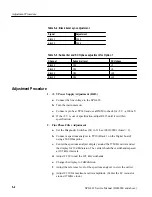
Page 138: ...ÁÁÁÁÁ C237 ÁÁÁÁÁÁÁÁ ÁÁÁÁÁÁÁÁ System Black ÁÁÁÁÁÁ ÁÁÁÁÁÁ TP9 ÁÁÁÁÁÁ ÁÁÁÁÁÁ C243 ÁÁÁÁÁÁÁ ÁÁÁÁÁÁÁ C244 Table 5 3 Fine phase filter check and sync tip adjustment ÁÁÁÁÁÁÁ ÁÁÁÁÁÁÁ Signal ÁÁÁÁÁÁÁ ÁÁÁÁÁÁÁ Adjustment ÁÁÁÁÁÁÁÁÁÁÁÁ ÁÁÁÁÁÁÁÁÁÁÁÁ Comments ÁÁÁÁÁÁÁ ÁÁÁÁÁÁÁ Black 1 ÁÁÁÁÁÁÁ ÁÁÁÁÁÁÁ R143 ÁÁÁÁÁÁÁÁÁÁÁÁ ÁÁÁÁÁÁÁÁÁÁÁÁ ÁÁÁÁÁÁÁ ÁÁÁÁÁÁÁ Black 2 ÁÁÁÁÁÁÁ ÁÁÁÁÁÁÁ R161 ÁÁÁÁÁÁÁÁÁÁÁÁ ÁÁÁÁÁÁÁÁÁÁÁÁ CH B1 on the 17...

Page 139: ...3 ÁÁÁÁÁÁÁÁ ÁÁÁÁÁÁÁÁ L14 Adjustment Procedure 1 5 V Power Supply Adjustment R415 a Connect the line voltage to the SPG 422 b Turn the instrument on c Connect a probe at TP140 and use a DMM to check for 5 V 100 mV d If the 5 V is out of specification adjust R415 until it is within specification 2 Fine Phase Filter Adjustment a Set the Diagnostic Switches S1 to 31 hex 001100001 closed 1 b Connect a s...

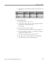
Page 140: ...7 ÁÁÁÁÁÁÁÁ ÁÁÁÁÁÁÁÁ System Black ÁÁÁÁÁÁ ÁÁÁÁÁÁ TP9 ÁÁÁÁÁÁ ÁÁÁÁÁÁ C243 ÁÁÁÁÁÁÁ ÁÁÁÁÁÁÁ C244 3 Fine Phase Filter Check a Keep the Diagnostic switch S1 in 31 hex b Connect TP19 27 MHz to channel 1 of the oscilloscope and channel 2 to TP10 Black 1 using 500 Ω scope probes c Invert channel 2 d Trigger on the signal from TP19 channel 1 e Check that the signal from TP10 lags that of TP19 by a nominal 2 2...

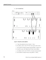
Page 141: ...nnect the equipment as shown in Figure 5 1 above b View Black 1 CH 1 on the 1781 PAL vectorscope waveform monitor c Use the SPG 422 front panel menu to change the Black 1 output to PAL d Adjust R143 gain on the Output board for proper sync amplitude e View Black 1 CH1 on the 1780 NTSC vectorscope waveform monitor f Use the SPG 422 front panel menu to change Black 1 to NTSC ...

Page 142: ...ÁÁÁÁÁÁ ÁÁÁÁÁÁÁÁÁÁÁ ÁÁÁÁÁÁÁÁÁÁÁ Option 1 only connect to CH B2 ÁÁÁÁÁÁ ÁÁÁÁÁÁ Black 6 ÁÁÁÁÁÁÁ ÁÁÁÁÁÁÁ R42 ÁÁÁÁÁÁÁÁÁÁÁ ÁÁÁÁÁÁÁÁÁÁÁ Option 1 only connect to CH B3 5 Black Burst Sin x x Adjustment a Connect the equipment as shown in Figure 5 1 b Use the SPG 422 front panel to output a PAL signal for Black 1 c View the Black 1 output CH A on the 1781 PAL vectorscope wave form monitor d Adjust C130 Sin x...

Page 143: ...nt panel menu to change Black 3 to output an NTSC signal g Check that the subcarrier level is 40 IREp p 2 IRE and the SCH Phase is 0 5 h Adjust C25 and L2 until both NTSC and PAL subcarrier specifications are met NOTE C25 has a gain effect on both NTSC and PAL subcarrier levels while L2 can be used to trade off gain between NTSC and PAL for their SCH perfor mance i Repeat procedure with Black 4 th...

Page 144: ......

Page 145: ...t and cost effective Tektronix maintains service centers around the world to provide quick turn around repair and recalibration services When this service is used even during the warranty period the instrument should be tagged and repackaged according to the instructions at the end of this section Preparation H Qualified Service Personnel Only H Read the Safety Summary and the Service Strategy H R...

Page 146: ...ng environment of the SPG 422 Under average conditions a preventive maintenance check should be performed at least once a year severe environment conditions such as high heat high humidity or dust may dictate a shorter time interval The instrument should be cleaned often enough to prevent dust or dirt from accumulating Dust accumulating in the instrument acts as an insulating blanket preventing pr...

Page 147: ...formance and reliability of the semiconductor components Static voltages of 1 kV to 30 kV are common in unprotected environments CAUTION Static discharge can damage or degrade many semiconductor components Table 6 1 Relative susceptibility levels Semiconductor classes Relative susceptibility levels ÁÁÁÁÁÁÁÁÁÁÁÁÁÁÁ ÁÁÁÁÁÁÁÁÁÁÁÁÁÁÁ ÁÁÁÁÁÁÁÁÁÁÁÁÁÁÁ MOS or CMOS microcircuits or discrete or linear mi c...

Page 148: ...s in areas that have a floor or work surface covering capable of generating a static charge Carpeted floors should be sprayed to reduce static problems Also nothing capable of generating or holding a static charge should be allowed on the work station surface 5 Keep the component leads shorted together whenever possible 6 Pick up the components by the body never by the leads 7 Do not slide the com...

Page 149: ... instrument is out of calibration or if there has been a component failure Once the type of failure has been determined proceed on to identify the functional area most likely at fault Visually inspect the suspect assembly for obvious defects Most commonly these will be broken or loose components improperly seated components overheated or burned components chafed insulation etc Repair or replace al...

Page 150: ... 800 number is a 24 hour service but service training specialists are only available between 8 am and 4 pm pacific coast time Tektronix maintains service centers worldwide These centers provide repair and calibration services for Tektronix instruments They can be contacted through your Tektronix field office or representative In addition US and Canadian customers can call 1 800 TEK WIDE 835 9433 f...

Page 151: ...replace ment part from Tektronix Circuit board assembly number Assembly name ÁÁÁÁÁÁÁÁ ÁÁÁÁÁÁÁÁ Front Panel ÁÁÁÁÁÁÁÁÁ ÁÁÁÁÁÁÁÁÁ A1 ÁÁÁÁÁÁÁÁ ÁÁÁÁÁÁÁÁ Digital ÁÁÁÁÁÁÁÁÁ ÁÁÁÁÁÁÁÁÁ A2 ÁÁÁÁÁÁÁÁ ÁÁÁÁÁÁÁÁ Output ÁÁÁÁÁÁÁÁÁ ÁÁÁÁÁÁÁÁÁ A3 ÁÁÁÁÁÁÁÁ ÁÁÁÁÁÁÁÁ EMI Filter ÁÁÁÁÁÁÁÁÁ ÁÁÁÁÁÁÁÁÁ A7 ÁÁÁÁÁÁÁÁ ÁÁÁÁÁÁÁÁ Option 1 ÁÁÁÁÁÁÁÁÁ ÁÁÁÁÁÁÁÁÁ A5 ÁÁÁÁÁÁÁÁ ÁÁÁÁÁÁÁÁ Option 2 ÁÁÁÁÁÁÁÁÁ ÁÁÁÁÁÁÁÁÁ A6 ÁÁÁÁÁÁÁÁ ÁÁÁÁÁÁÁÁ ÁÁÁ...

Page 152: ...field office or representative However many common electric parts are available through local sources Using a local source where possible will eliminate shipping delays Changes to Tektronix instruments are sometimes made to accommodate improved components as they become available and to improve circuit performance Therefore it is important to include the following information when ordering parts 1...

Page 153: ...internal genlock this LED should never be on ÁÁÁÁÁÁ ÁÁÁÁÁÁ ÁÁÁÁÁÁ Digital ÁÁÁ ÁÁÁ ÁÁÁ DS2 ÁÁÁÁÁÁÁÁÁÁ ÁÁÁÁÁÁÁÁÁÁ ÁÁÁÁÁÁÁÁÁÁ 108 Loop Unlocked ÁÁÁÁÁÁÁÁÁÁÁÁÁÁÁÁÁÁ ÁÁÁÁÁÁÁÁÁÁÁÁÁÁÁÁÁÁ ÁÁÁÁÁÁÁÁÁÁÁÁÁÁÁÁÁÁ The 108 PLL is outside of its 50 kHz pull in range If DS1 and DS4 are also on wait for the crystal to warm up before continuing troubleshoot ing Otherwise there is a problem in the 108 MHz oscillator ci...

Page 154: ...ÁÁÁÁÁÁ ÁÁÁÁÁÁÁÁ ÁÁÁÁÁÁÁÁ ÁÁÁÁÁÁÁÁ ÁÁÁÁÁÁÁÁ ÁÁÁÁÁÁÁÁ RAM diagnostic ÁÁÁÁÁÁÁÁÁÁÁÁÁÁÁÁÁÁÁ ÁÁÁÁÁÁÁÁÁÁÁÁÁÁÁÁÁÁÁ ÁÁÁÁÁÁÁÁÁÁÁÁÁÁÁÁÁÁÁ ÁÁÁÁÁÁÁÁÁÁÁÁÁÁÁÁÁÁÁ ÁÁÁÁÁÁÁÁÁÁÁÁÁÁÁÁÁÁÁ ÁÁÁÁÁÁÁÁÁÁÁÁÁÁÁÁÁÁÁ ÁÁÁÁÁÁÁÁÁÁÁÁÁÁÁÁÁÁÁ ÁÁÁÁÁÁÁÁÁÁÁÁÁÁÁÁÁÁÁ ÁÁÁÁÁÁÁÁÁÁÁÁÁÁÁÁÁÁÁ Read write test of all RAMs This routine tests 1 Serial Color Bar RAM U26 U27 2 Serial Color Bar Coprocessor RAM U42 U43 3 Read back registers on the Opt...

Page 155: ...lt If a readback compare is in error the routine pre maturely returns with an error number At the end of the routine the backlight blinks indicating that all tests have passed The error number is NOT programmed to display anything at this time How ever if no errors have occurred then the routine will not have quit early and the Backlight will blink ÁÁÁÁ ÁÁÁÁ ÁÁÁÁ ÁÁÁÁ ÁÁÁÁ ÁÁÁÁ ÁÁÁÁ ÁÁÁÁ ÁÁÁÁ C U ...

Page 156: ...nstrument only Wait for a button to be pressed If LEFT_BUTTON or RIGHT_BUTTON is selected to update value and write the test value to the contrast DAC ÁÁÁÁ ÁÁÁÁ ÁÁÁÁ ÁÁÁÁ ÁÁÁÁ ÁÁÁÁ ÁÁÁÁ C U ÁÁÁÁÁ ÁÁÁÁÁ ÁÁÁÁÁ XoooXoXX ÁÁÁÁÁÁÁÁ ÁÁÁÁÁÁÁÁ ÁÁÁÁÁÁÁÁ Genlock FPGA diagnos tics ÁÁÁÁÁÁÁÁÁÁÁÁÁÁÁÁÁÁÁ ÁÁÁÁÁÁÁÁÁÁÁÁÁÁÁÁÁÁÁ ÁÁÁÁÁÁÁÁÁÁÁÁÁÁÁÁÁÁÁ This routine downloads a new configuration file to the genlock control...

Page 157: ...uate protection If the original packaging is not available or is unfit for use repackage the instrument as follows 1 Obtain a corrugated cardboard carton whose inside dimensions are at least six inches greater than the dimensions of the instrument to allow room for cushioning The shipping carton should have a test strength of at least 275 pounds 2 Surround the instrument with polyethylene sheeting...

Page 158: ...Maintenance 6 14 SPG 422 Service Manual B034000 and above ...

Page 159: ......

Page 160: ...ted and CSA certified Cords for use in areas other than North America are approved by at least one test house acceptable in the country to which the product is shipped Power cord part numbers are shown on the Accessories pull out Option 1 adds four additional analog black outputs to the two outputs that are standard on the SPG 422 This is accomplished by adding a board to the SPG 422 and can be do...

Page 161: ...and above Ordering Any of these options can be ordered with the SPG 422 In addition these items are available from your nearest Tektronix field office or distributor Be sure to include both the name and number of any Field Upgrades Kits ordered ...

Page 162: ......

Page 163: ...llowing information in your order H Part number H Instrument type or model number H Instrument serial number H Instrument modification number if applicable If you order a part that has been replaced with a different or improved part your local Tektronix field office or representative will contact you concerning any change in part number Change information if any is located at the rear of this manu...

Page 164: ...ber at which the part was discontinued No entry indicates the part is good for all serial numbers 5 Name description An item name is separated from the description by a colon Because of space limitations an item name may sometimes appear as incomplete Use the U S Federal Catalog handbook H6 1 for further item name identification 6 Mfr code This indicates the code number of the actual manufacturer ...

Page 165: ... 10523 TK2058 TDK CORPORATION OF AMERICA 1600 FEEHANVILLE DRIVE MOUNT PROSPECT IL 60056 TK2073 TOKYO AMERICA INC 565 W GULF ROAD ARLINGTON HEIGHTS IL 60005 TK2319 COLLMER 14368 PROTON RD DALLAS TX 75244 TK2469 UNITREK CORPORATION 3000 LEWIS CLARK WAY SUITE 2 VANCOUVER WA 98601 TK2519 ALLIANCE SEMICONDUCTOR 3099 N FIRST ST SAN JOSE CA 95134 2006 TK2598 MAXIM ASIC 14150 SW KARL BRAUN DRIVE BEAVERTON...

Page 166: ... 3915 17856 SILICONIX INC 2201 LAURELWOOD RD SANTA CLARA CA 95054 1516 19615 ALLEN AVIONICS INC 255 EAST 2ND ST P O BOX 350 MINEOLA NY 11501 3503 18565 CHOMERICS INC 77 DRAGON COURT WOBURN MA 01880 2W944 PAPST MECHATRONIC CORP AQUIDNECK INDUSTRIAL PK NEWPORT RI 02840 22526 BERG ELECTRONICS INC DUPONT 857 OLD TRAIL RD ETTERS PA 17319 24165 SPRAGUE ELECTRIC CO 267 LOWELL ROAD HUDSON NH 03051 24355 A...

Page 167: ...TA CLARA CA 95051 61935 SCHURTER INC 1016 CLEGG COURT PETALUMA CA 94952 1152 62104 CALIFORNIA EASTERN LABORATORIES INC 4590 PATRICK HENRY DR SANTA CLARA CA 95054 3309 62643 UNITED CHEMICON INC 9801 W HIGGINS ST SUITE 430 ROSEMONT IL 60018 4771 65786 CYPRESS SEMICONDUCTOR CORP 3901 N FIRST ST SAN JOSE CA 95134 1506 66958 SGS THOMSON MICROELECTRONICS 1000 E BELL RD PHOENIX AZ 85022 2649 67183 ALTERA...

Page 168: ...74 2744 00 CA ASSY SP ELEC 34 28 AWG 3 25 L RIBBON 53387 174 2744 00 A1S1 260 2671 00 SWITCH PUSH SPST MOM NO 100 GRM FRC COND RUBBER CONTACTS GRN LED W KEYCAP TK2635 SKECFL 366 0779 00 PUSH BUTTON PUSH BUTTON KEYTOP W LENS VM700A TK2635 SCGRY1 A1S2 260 2671 00 SWITCH PUSH SPST MOM NO 100 GRM FRC COND RUBBER CONTACTS GRN LED W KEYCAP TK2635 SKECFL 366 0779 00 PUSH BUTTON PUSH BUTTON KEYTOP W LENS ...

Page 169: ...ECFL 366 0779 00 PUSH BUTTON PUSH BUTTON KEYTOP W LENS VM700A TK2635 SCGRY1 A1S12 260 2671 00 SWITCH PUSH SPST MOM NO 100 GRM FRC COND RUBBER CONTACTS GRN LED W KEYCAP TK2635 SKECFL 366 0779 00 PUSH BUTTON PUSH BUTTON KEYTOP W LENS VM700A TK2635 SCGRY1 A1S14 260 2671 00 SWITCH PUSH SPST MOM NO 100 GRM FRC COND RUBBER CONTACTS GRN LED W KEYCAP TK2635 SKECFL 366 0779 00 PUSH BUTTON PUSH BUTTON KEYTO...

Page 170: ...6 04222 12065E104ZAT3A A2C19 283 5098 00 CAP FXD CER MLC 0 1UF 80 20 50V Z5U 1206 04222 12065E104ZAT3A A2C20 283 5098 00 CAP FXD CER MLC 0 1UF 80 20 50V Z5U 1206 04222 12065E104ZAT3A A2C21 283 5098 00 CAP FXD CER MLC 0 1UF 80 20 50V Z5U 1206 04222 12065E104ZAT3A A2C22 283 5098 00 CAP FXD CER MLC 0 1UF 80 20 50V Z5U 1206 04222 12065E104ZAT3A A2C24 290 0963 00 CAP FXD ALUM 220UF 50 20 25WVDC 10 X12M...

Page 171: ...P FXD CER MLC 0 1UF 80 20 50V Z5U 1206 04222 12065E104ZAT3A A2C70 283 5098 00 CAP FXD CER MLC 0 1UF 80 20 50V Z5U 1206 04222 12065E104ZAT3A A2C71 283 5098 00 CAP FXD CER MLC 0 1UF 80 20 50V Z5U 1206 04222 12065E104ZAT3A A2C72 283 5098 00 CAP FXD CER MLC 0 1UF 80 20 50V Z5U 1206 04222 12065E104ZAT3A A2C73 283 5098 00 CAP FXD CER MLC 0 1UF 80 20 50V Z5U 1206 04222 12065E104ZAT3A A2C74 283 5098 00 CA...

Page 172: ...P FXD CER MLC 0 1UF 80 20 50V Z5U 1206 04222 12065E104ZAT3A A2C110 283 5003 00 CAP FXD CER MLC 0 01UF 10 50V X7R 1206 TK2058 C3216X7R1H103K A2C111 283 5098 00 CAP FXD CER MLC 0 1UF 80 20 50V Z5U 1206 04222 12065E104ZAT3A A2C112 290 5037 01 CAP FXD ALUM 10UF 20 35V 5 7 H X 5 DIA MM 62643 MVK35VC10RME60T A2C113 283 5098 00 CAP FXD CER MLC 0 1UF 80 20 50V Z5U 1206 04222 12065E104ZAT3A A2C119 283 5003...

Page 173: ...D CER MLC 0 1UF 80 20 50V Z5U 1206 04222 12065E104ZAT3A A2C176 283 5265 00 CAP FXD CER MLC 0 0033UF 5 50V NPO 1206 04222 12065A332JAT1A A2C177 283 5106 00 CAP FXD CER MLC 470PF 5 100V NPO 1206 04222 12061A471JAT1A A2C178 283 5189 00 CAP FXD CER MLC 220PF 5 100V NPO 1206 04222 12061A221JAT1A A2C179 283 5197 00 CAP FXD CER MLC 330PF 5 100V NPO 1206 04222 12061A331JAT1A A2C180 283 5189 00 CAP FXD CER...

Page 174: ...C215 283 5098 00 CAP FXD CER MLC 0 1UF 80 20 50V Z5U 1206 04222 12065E104ZAT3A A2C216 283 5098 00 CAP FXD CER MLC 0 1UF 80 20 50V Z5U 1206 04222 12065E104ZAT3A A2C217 283 5098 00 CAP FXD CER MLC 0 1UF 80 20 50V Z5U 1206 04222 12065E104ZAT3A A2C218 283 5098 00 CAP FXD CER MLC 0 1UF 80 20 50V Z5U 1206 04222 12065E104ZAT3A A2C219 283 5098 00 CAP FXD CER MLC 0 1UF 80 20 50V Z5U 1206 04222 12065E104ZAT...

Page 175: ...0V Z5U 1206 04222 12065E104ZAT3A A2C256 283 5098 00 CAP FXD CER MLC 0 1UF 80 20 50V Z5U 1206 04222 12065E104ZAT3A A2C257 283 5098 00 CAP FXD CER MLC 0 1UF 80 20 50V Z5U 1206 04222 12065E104ZAT3A A2C258 283 5003 00 CAP FXD CER MLC 0 01UF 10 50V X7R 1206 TK2058 C3216X7R1H103K A2C259 283 5003 00 CAP FXD CER MLC 0 01UF 10 50V X7R 1206 TK2058 C3216X7R1H103K A2C260 283 5003 00 CAP FXD CER MLC 0 01UF 10 ...

Page 176: ...V 0 74VF 4NS 2 0PF SER PAIR 27014 MMBD1203 A2CR6 152 5018 00 DIODE SIG ULTRA FAST 100V 0 74VF 4NS 2 0PF SER PAIR 27014 MMBD1203 A2CR7 152 5018 00 DIODE SIG ULTRA FAST 100V 0 74VF 4NS 2 0PF SER PAIR 27014 MMBD1203 A2CR8 152 5018 00 DIODE SIG ULTRA FAST 100V 0 74VF 4NS 2 0PF SER PAIR 27014 MMBD1203 A2CR9 152 5018 00 DIODE SIG ULTRA FAST 100V 0 74VF 4NS 2 0PF SER PAIR 27014 MMBD1203 A2CR10 152 5018 0...

Page 177: ...NN HDR PCB MALE STR 2 X 5 0 1 CTR 0 365 H X 0 112 TAIL SHRD 4 SIDES MIL PLZ 30 GOLD 53387 2510 6002UB A2J10 131 3270 00 CONN HDR PCB MALE STR 1 X 2 0 1 CTR 0 295 MLG X 0 140 TAIL TIN PLZ WALL W FRICTION LOCK 00779 640456 2 A2J11 131 4183 00 CONN HDR PCB MALE STR 2 X 7 0 1 CTR 0 365 H X 0 112 TAIL SHRD 4 SIDES CTR PLZ 30 GOLD 53387 2514 6002UB A2J12 131 4530 00 CONN HDR PCB MALE STR 1 X 3 0 1 CTR 0...

Page 178: ...AL SHIELDED 560NH IDC 440 MA RDC 0 51 OHM Q 50 SRF 180 MHZ TK2058 ACL3225S R56KT A2P1 131 0993 02 BUS CONDUCTOR SHUNT ASSEMBLY RED 00779 1 850100 O A2P2 131 0993 02 BUS CONDUCTOR SHUNT ASSEMBLY RED 00779 1 850100 O A2Q3 151 5072 00 XSTR PWR MOS N CH 50V 0 045 OHM LOGIC 17856 SMD25N05 45L A2Q5 151 5034 00 XSTR SIG BIPOLAR NPN 14V 50MA 1 5GHZ AMPL 62104 NE73433 T1B 2S A2Q6 151 5008 00 XSTR SIG BIPOL...

Page 179: ...R41 321 5030 00 RES FXD THICK FILM 10 0K OHM 1 0 125W TC 100 PPM 50139 BCK1002FT A2R42 321 5030 00 RES FXD THICK FILM 10 0K OHM 1 0 125W TC 100 PPM 50139 BCK1002FT A2R43 321 5029 00 RES FXD THICK FILM 8 25K OHM 1 0 125W TC 100 PPM 50139 BCK8251FT A2R44 321 5027 00 RES FXD THICK FILM 5 62K OHM 1 0 125W TC 100 PPM 50139 BCK5621FT A2R45 321 5027 00 RES FXD THICK FILM 5 62K OHM 1 0 125W TC 100 PPM 501...

Page 180: ...M 1 0 125W TC 100 PPM 57668 MCR18FXEA1M A2R81 321 5026 00 RES FXD THICK FILM 4 75K OHM 1 0 125W TC 100 PPM 50139 BCK4751FT A2R82 321 5024 00 RES FXD THICK FILM 3 32K OHM 1 0 125W TC 100 PPM 50139 BCK3321FT A2R83 321 5030 00 RES FXD THICK FILM 10 0K OHM 1 0 125W TC 100 PPM 50139 BCK1002FT A2R84 321 5030 00 RES FXD THICK FILM 10 0K OHM 1 0 125W TC 100 PPM 50139 BCK1002FT A2R85 321 5019 00 RES FXD TH...

Page 181: ... 0 125W TC 100 PPM 50139 BCK2211FT A2R119 321 5022 00 RES FXD THICK FILM 2 21K OHM 1 0 125W TC 100 PPM 50139 BCK2211FT A2R120 321 5034 00 RES FXD THICK FILM 22 1K OHM 1 0 125W TC 100 PPM 50139 BCK2212FT A2R121 321 5018 00 RES FXD THICK FILM 1 0K OHM 1 0 125W TC 100 PPM 50139 BCK1001FT A2R122 321 5018 00 RES FXD THICK FILM 1 0K OHM 1 0 125W TC 100 PPM 50139 BCK1001FT A2R128 321 5045 00 RES FXD THIC...

Page 182: ...FXD THICK FILM 10 OHM 1 0 125W TC 100 PPM 59124 RK73H2B10R0FT A2R186 321 5004 00 RES FXD THICK FILM 22 1 OHM 1 0 125W TC 100 PPM 57668 MCR18FWEA22E1 A2R187 321 5030 00 RES FXD THICK FILM 10 0K OHM 1 0 125W TC 100 PPM 50139 BCK1002FT A2R188 321 5036 00 RES FXD THICK FILM 33 2K OHM 1 0 125W TC 100 PPM 50139 BCK3322FT A2R189 321 5018 00 RES FXD THICK FILM 1 0K OHM 1 0 125W 50139 BCK1001FT A2R190 321 ...

Page 183: ...25W TC 100 50139 BCK3320FT A2R1003 321 5014 00 RES FXD THICK FILM 475 OHM 1 0 125W TC 100 50139 BCK4750FT A2R1004 321 5012 00 RES FXD THICK FILM 332 OHM 1 0 125W TC 100 50139 BCK3320FT A2R1005 321 5012 00 RES FXD THICK FILM 332 OHM 1 0 125W TC 100 50139 BCK3320FT A2R1006 321 5012 00 RES FXD THICK FILM 332 OHM 1 0 125W TC 100 50139 BCK3320FT A2R1007 321 5012 00 RES FXD THICK FILM 332 OHM 1 0 125W T...

Page 184: ...46 00 RES FXD THICK FILM 82 5 OHM 1 0 125W TC 100 PPM 50139 BCK82R5FT A2R1044 321 5017 00 RES FXD THICK FILM 825 OHM 1 0 125W TC 100 50139 BCK8250FT A2R1045 321 5017 00 RES FXD THICK FILM 825 OHM 1 0 125W TC 100 50139 BCK8250FT A2R1046 321 5017 00 RES FXD THICK FILM 825 OHM 1 0 125W TC 100 50139 BCK8250FT A2R1047 321 5005 00 RES FXD THICK FILM 27 4 OHM 1 0 125W TC 100 PPM 57668 MCR18EZHFW 27E4 A2R...

Page 185: ...21 5030 00 RES METAL FILM 10 0K OHM 1 0 2W TC 100 PPM 50139 BCK1002FT A2S1 260 1721 00 SWITCH ROCKER 8 SPST 125MA 30VDC 81073 76SB08S A2TP1 214 4085 00 TERM TEST POINT 0 070 ID 0 220 H 0 063 DIAP CB 0 015 X 0 032 BRASS W RED NYLON COLLAR 26364 104 01 02 A2TP2 214 4085 00 TERM TEST POINT 0 070 ID 0 220 H 0 063 DIAP CB 0 015 X 0 032 BRASS W RED NYLON COLLAR 26364 104 01 02 A2TP3 214 4085 00 TERM TES...

Page 186: ... BFR DRIVER 3 STATE 0JR04 TC74HCT244AFW E A2U9 163 0298 00 IC DGTL CMOS PLD EEPLD 7128E 128 M C 64 I O 4 IN 15NS TK0198 163029800 A2U10 163 1322 01 IC MEMORY CMOS EPROM 256K X 8 150NS PRGM TK0198 163 1322 00 A2U11 163 1323 00 IC MEMORY CMOS EPROM 256K X 8 150NS PRGM TK0198 163 1323 00 136 1223 00 SOCKET PLCC PCB 32 POS 0 05 CTR 0 86 X 0 740 WIDE 00779 821665 1 A2U12 156 0878 00 IC MISC TTL INTERFA...

Page 187: ...FR OCTAL BFR DRIVER 3 STATE 0JR04 TC74HCT244AFW E A2U39 156 5071 01 IC DIGITAL HCTCMOS TRANSCEIVER OCTAL 3 STATE 0JR04 TC74HCT245AFW E A2U40 156 5071 01 IC DIGITAL HCTCMOS TRANSCEIVER OCTAL 3 STATE 0JR04 TC74HCT245AFW E A2U41 156 5164 01 IC DIGITAL FTTL GATES QUAD 2 INPUT NAND OC 01295 SN74F38DR A2U42 156 6794 00 IC MEMORY CMOS SRAM 32K X 8 15NS 5C2568 SOJ28 300 TK2519 AS7C256 15JC A2U43 156 6794 ...

Page 188: ...P FLOP DUAL D TYPE METASTABLE IMMUNITY 1CH66 N74F5074D A2U91 163 0295 00 IC DIGITAL CMOS PLD EEPLD 7032 32 M C 32 I O 4IN 7 5NS 80009 163 0295 00 A2U92 156 6260 00 IC DIGITAL FCTCMOS BFR OCTAL 3 STATE 61772 IDT74FCT244ATSO A2U93 156 5055 01 IC DIGITAL FTTL FLIP FLOP DUAL D TYPE 01295 SN74F74DR A2U94 156 5506 00 IC DIGITAL FTTL RGTR QUAD 2 PORT 04713 MC74F399D A2U95 156 5324 01 IC DIGITAL ECL TRANS...

Page 189: ...7 321 5051 00 RES FXD THICK FILM 0 OHM 1 0 125W TC 100 PPM 09969 CRCW1206 JUMPER A2W8 321 5051 00 RES FXD THICK FILM 0 OHM 1 0 125W TC 100 PPM 09969 CRCW1206 JUMPER A2W9 321 5051 00 RES FXD THICK FILM 0 OHM 1 0 125W TC 100 PPM 09969 CRCW1206 JUMPER A2W10 321 5051 00 RES FXD THICK FILM 0 OHM 1 0 125W TC 100 PPM 09969 CRCW1206 JUMPER A2Y1 119 1897 00 OSCILLATOR RF XTAL CONTROLLED 8 00MHZ 0 01 61429 ...

Page 190: ... T D A2A1Q1 151 0429 00 XSTR PWR BIPOLAR PNP 60V 4 0A 1 0MHZ AMPL DARLINGTON 04713 MJE700 A2A1Q2 151 5035 00 XSTR SIG BIPOLAR NPN 25V 30MA 650MHZ AMPL 04713 MMBTH10LT1 A2A1Q3 151 5035 00 XSTR SIG BIPOLAR NPN 25V 30MA 650MHZ AMPL 04713 MMBTH10LT1 A2A1R1 321 5049 00 RES FXD THICK FILM 1M OHM 1 0 125W TC 100 PPM 57668 MCR18FXEA1M A2A1R2 321 5015 00 RES FXD THICK FILM 562 OHM 1 0 125W TC 100 50139 BCK...

Page 191: ...UF 80 20 50V Z5U 1206 04222 12065E104ZAT3A A3C17 283 5098 00 CAP FXD CER MLC 0 1UF 80 20 50V Z5U 1206 04222 12065E104ZAT3A A3C18 283 5098 00 CAP FXD CER MLC 0 1UF 80 20 50V Z5U 1206 04222 12065E104ZAT3A A3C19 283 5098 00 CAP FXD CER MLC 0 1UF 80 20 50V Z5U 1206 04222 12065E104ZAT3A A3C20 283 5098 00 CAP FXD CER MLC 0 1UF 80 20 50V Z5U 1206 04222 12065E104ZAT3A A3C21 283 5098 00 CAP FXD CER MLC 0 1...

Page 192: ...1 283 5098 00 CAP FXD CER MLC 0 1UF 80 20 50V Z5U 1206 04222 12065E104ZAT3A A3C72 283 5098 00 CAP FXD CER MLC 0 1UF 80 20 50V Z5U 1206 04222 12065E104ZAT3A A3C73 283 5098 00 CAP FXD CER MLC 0 1UF 80 20 50V Z5U 1206 04222 12065E104ZAT3A A3C74 283 5098 00 CAP FXD CER MLC 0 1UF 80 20 50V Z5U 1206 04222 12065E104ZAT3A A3C75 283 5098 00 CAP FXD CER MLC 0 1UF 80 20 50V Z5U 1206 04222 12065E104ZAT3A A3C7...

Page 193: ... MLC 1UF 80 20 25V Y5V 1206 04222 12063G105ZAT1A A3C110 283 5201 00 CAP FXD CER MLC 33PF 5 100V NPO 1206 04222 12061A330JAT1A A3C111 283 5201 00 CAP FXD CER MLC 33PF 5 100V NPO 1206 04222 12061A330JAT1A A3C112 283 5201 00 CAP FXD CER MLC 33PF 5 100V NPO 1206 04222 12061A330JAT1A A3C113 283 5201 00 CAP FXD CER MLC 33PF 5 100V NPO 1206 04222 12061A330JAT1A A3C114 283 5267 00 CAP FXD CER MLC 1UF 80 2...

Page 194: ...CAP FXD CER MLC 0 1UF 80 20 50V Z5U 1206 04222 12065E104ZAT3A A3C150 283 5098 00 CAP FXD CER MLC 0 1UF 80 20 50V Z5U 1206 04222 12065E104ZAT3A A3C151 283 5098 00 CAP FXD CER MLC 0 1UF 80 20 50V Z5U 1206 04222 12065E104ZAT3A A3C152 283 5098 00 CAP FXD CER MLC 0 1UF 80 20 50V Z5U 1206 04222 12065E104ZAT3A A3C153 283 5098 00 CAP FXD CER MLC 0 1UF 80 20 50V Z5U 1206 04222 12065E104ZAT3A A3C154 283 509...

Page 195: ...T3A A3C1019 283 5098 00 CAP FXD CER MLC 0 1UF 80 20 50V Z5U 1206 04222 12065E104ZAT3A A3C1020 283 5098 00 CAP FXD CER MLC 0 1UF 80 20 50V Z5U 1206 04222 12065E104ZAT3A A3C1021 283 5098 00 CAP FXD CER MLC 0 1UF 80 20 50V Z5U 1206 04222 12065E104ZAT3A A3C1022 283 5098 00 CAP FXD CER MLC 0 1UF 80 20 50V Z5U 1206 04222 12065E104ZAT3A A3C1023 283 5098 00 CAP FXD CER MLC 0 1UF 80 20 50V Z5U 1206 04222 1...

Page 196: ... A3K1 148 0255 00 RELAY LATCHING DPDT 61529 DS2E M DC5V A3L1 108 1557 00 INDUCTOR FXD CUSTOM SIGNAL 15UH 10 IDC 5 0 0JR03 108 1557 00 A3L2 108 1557 00 INDUCTOR FXD CUSTOM SIGNAL 15UH 10 IDC 5 0 0JR03 108 1557 00 A3L3 108 0550 00 INDUCTOR FXD CUSTOM SIGNAL 89NH Q 39 50MHZ ON FORM 276 0153 00 0JR03 108 0550 00 A3L4 108 0550 00 INDUCTOR FXD CUSTOM SIGNAL 89NH Q 39 50MHZ ON FORM 276 0153 00 0JR03 108 ...

Page 197: ...MMBT3904LT1 A3R1 321 5006 00 RES FXD THICK FILM 100 OHM 1 0 125W TC 100 50139 BCK1000FT A3R2 321 5008 00 RES FXD THICK FILM 150 OHM 1 0 125W TC 100 50139 BCK1500FT A3R3 321 5006 00 RES FXD THICK FILM 100 OHM 1 0 125W TC 100 50139 BCK1000FT A3R4 321 5008 00 RES FXD THICK FILM 150 OHM 1 0 125W TC 100 50139 BCK1500FT A3R5 321 5006 00 RES FXD THICK FILM 100 OHM 1 0 125W TC 100 50139 BCK1000FT A3R6 321...

Page 198: ...R58 321 5032 00 RES FXD THICK FILM 15 0K OHM 1 0 125W TC 100 PPM 50139 BCK1502FT A3R59 321 5050 00 RES FXD THICK FILM 33 2 OHM 1 0 125W TC 100 PPM 57668 MCR18FWEA33E2 A3R60 321 5050 00 RES FXD THICK FILM 33 2 OHM 1 0 125W TC 100 PPM 57668 MCR18FWEA33E2 A3R61 321 5047 00 RES FXD THICK FILM 100K OHM 1 0 125W TC 100 PPM 50139 BCK1003FT A3R62 321 5016 00 RES FXD THICK FILM 681 OHM 1 0 125W TC 100 5013...

Page 199: ...5K OHM 1 0 125W TC 100 PPM 50139 BCK8251FT A3R100 321 5029 00 RES FXD THICK FILM 8 25K OHM 1 0 125W TC 100 PPM 50139 BCK8251FT A3R101 321 5022 00 RES FXD THICK FILM 2 21K OHM 1 0 125W TC 100 PPM 50139 BCK2211FT A3R102 321 5019 00 RES FXD THICK FILM 1 21K OHM 1 0 125W TC 100 PPM 50139 BCK1211FT A3R103 321 5022 00 RES FXD THICK FILM 2 21K OHM 1 0 125W TC 100 PPM 50139 BCK2211FT A3R104 321 5018 00 RE...

Page 200: ... 1 0 125W TC 100 50139 BCK3320FT A3R158 322 3085 07 RES FXD METAL FILM 75 OHM 0 1 0 2W TC 25 PPM 91637 CCF502 C75ROOBT A3R159 321 5017 00 RES FXD THICK FILM 825 OHM 1 0 125W TC 100 50139 BCK8250FT A3R160 321 5113 00 RES FXD THICK FILM 75 OHM 1 0 125W TC 100 PPM 56845 CRCW1206 75ROFT A3R161 311 5033 00 RES VAR TRMR CERMET 500 OHM 25 0 25W 4MM SQ TOP TK2073 G4DT501M A3R162 321 5018 00 RES FXD THICK ...

Page 201: ...0 OHM 1 0 125W TC 100 50139 BCK1000FT A3R1008 321 5000 00 RES FXD THICK FILM 10 OHM 1 0 125W TC 100 PPM 59124 RK73H2B10R0FT A3R1009 321 5009 00 RES FXD THICK FILM 182 OHM 1 0 125W TC 100 50139 BCK1820FT A3R1010 321 5050 00 RES FXD THICK FILM 33 2 OHM 1 0 125W TC 100 PPM 57668 MCR18FWEA33E2 A3R1011 321 5050 00 RES FXD THICK FILM 33 2 OHM 1 0 125W TC 100 PPM 57668 MCR18FWEA33E2 A3R1012 321 5050 00 R...

Page 202: ... SRAM 32K X 8 25NS 80009 156627401 A3U24 163 0292 00 IC DGTL CMOS PLD EEPLD 7128E 128 M C 64I O 4 IN 15NS 80009 163 0292 00 A3U25 156 5514 00 IC DIGITAL FTTL FLIP FLOP OCTAL D TYPE WITH ENABLE 01295 SN74F377ADW A3U26 156 5052 01 IC DIGITAL FTTL GATE HEX INV 01295 SN74F04DR A3U27 156 5147 01 IC DIGITAL HCTCMOS FLIP FLOP OCTAL D TYPE CLEAR 01295 SN74HCT273DWR A3U28 156 5147 01 IC DIGITAL HCTCMOS FLI...

Page 203: ... 01 IC LINEAR BIPOLAR OP AMP CURRENTFEEDBACK 65MHZ 24355 AD810AR REEL A3U51 156 6643 00 IC LINEAR BIPOLAR OP AMP 50MHZ UNITYGAIN STABLE 24355 AD847JR A3U52 163 0291 00 IC MEMORY CMOS EPROM 256K X 8 150NS 80009 163029100 A3U53 160 9926 00 IC MEMORY CMOS EPROM 256K X 8 150NS 80009 160992600 A3U54 160 9924 00 IC MEMORY CMOS EPROM 128K X8 120NS OTP 80009 160992400 A3U55 160 9925 00 IC MEMORY CMOS 3276...

Page 204: ...0 CAP FXD ALUM 1000UF 20 35V 12 5 X 30MM 0 492 X 1 180 0H1N5 CEEFM1V102M7 A4C160 290 1315 00 CAP FXD ALUM 47UF 20 35V ESR 0 34 OHM 100KHZ 20C 6X11MM LOW IMP 55680 UPL1V470MEH1TD A4C162 290 1315 00 CAP FXD ALUM 47UF 20 35V ESR 0 34 OHM 100KHZ 20C 6X11MM LOW IMP 55680 UPL1V470MEH1TD A4C170 290 1315 00 CAP FXD ALUM 47UF 20 35V ESR 0 34 OHM 100KHZ 20C 6X11MM LOW IMP 55680 UPL1V470MEH1TD A4C172 290 131...

Page 205: ...0 100 X 04222 SA71C102KAA A4C621 281 0772 00 CAP FXD CER MLC 4700PF 10 100V 0 100 X 04222 SA71C472KAA A4C650 281 0563 00 CAP FXD CER MLC 0 47UF 20 50V 0 150 X 0 290 04222 SA305E474MAA A4C656 290 1309 00 CAP FXD AL 100UF 20 63V 10 X 20MM RADIAL 105 DEG L0W Z T A 0H1N5 CEEFM1J101M6 T4 A4C657 281 0775 01 CAP FXD CER MCL 0 1UF 20 50V Z5U 0 170 04222 SA75E104MAA A4C700 285 1421 00 CAP FXD PLASTIC 1 0UF...

Page 206: ...ON 71400 MDL 1 MOUNTING PARTS 204 0906 00 BODY FUSEHOLDER 3AG 5 X 20MM FUSES 61935 TYPE FAU 031 35 END MOUNTING PARTS A4FL950 119 3835 00 FILTER RFI 3A 250V 400HZ W PC TERMINALS 0GV52 FN 326 3 02 A4J160 131 3364 00 CONN HDR PCB MALE STR 2 X 17 0 1 CTR 0 365D 53387 2534 6002UB A4J370 131 3270 00 CONN HDR PCB MALE STR 1 X 2 0 1 CTR 00779 640456 2 A4H5 214 2953 00 HEAT SINK SEMIC TRANSISTOR TO 220 VE...

Page 207: ... RES FXD 0 27 OHM 5 1W MI 75042 BW 20 R2700J A4R314 322 3291 00 RES FXD METAL FILM 10 5K OHM 1 0 2W TC 100 PPM 57668 CRB20 FXE 10K5 A4R315 322 3235 00 RES FXD METAL FILM 2 74K OHM 1 0 2W TC 100 57668 CRB20 FXE 2K74 A4R316 322 3168 00 RES FXD METAL FILM 549 OHM 1 0 2W TC 100 PPM 91637 CCF50 5490F R36 A4R320 315 0101 00 RES FXD FILM 100 OHM 5 0 25W MI TK1727 SFR25 2322 181 A4R415 311 2231 00 RES VAR...

Page 208: ...00 PPM 57668 CRB20T68EFX2001 A4RT820 307 0746 00 RES THERMAL 5 OHM 10 7A DEG C 15454 SG200 S STRAI A4S930 260 2443 00 SWITCH PWR DPDT PUSH PUSH ALT ACT PC PINS 6A 250VAC 1A 100VDC 36A AC SURGE 31918 NE18 00 EE N 47 A4T1 120 1897 00 XFMR RF PWR SWITCHING 70KHZ PRI 254V SEC 100V 0 1A 75498 129 0122 EE A4T2 120 1889 00 TRANSFORMER RF TOROID 1 1 150UH 10 0JR03 120 1889 00 A4U150 156 3633 00 IC LINEAR ...

Page 209: ...22 12065E104ZAT3A A5C16 283 5098 00 CAP FXD CER MLC 0 1UF 80 20 50V Z5U 1206 04222 12065E104ZAT3A A5C17 283 5098 00 CAP FXD CER MLC 0 1UF 80 20 50V Z5U 1206 04222 12065E104ZAT3A A5C23 283 5196 00 CAP FXD CER MLC 47PF 5 100V NPO 1206 04222 12061A470JAT1A A5C24 283 5098 00 CAP FXD CER MLC 0 1UF 80 20 50V Z5U 1206 04222 12065E104ZAT3A A5C25 281 5012 00 CAP VAR CER 5 40PF 25V N750 500PPM C SINGLE TURN...

Page 210: ... 1206 04222 12061A71JAT1A A5C60 283 5238 00 CAP FXD CER MLC 150PF 5 100V NPO 1206 04222 12061A151JAT1A A5C61 283 5196 00 CAP FXD CER MLC 47PF 5 100V NPO 1206 04222 12061A470JAT1A A5C62 283 5098 00 CAP FXD CER MLC 0 1UF 80 20 50V Z5U 1206 04222 12065E104ZAT3A A5C63 281 5012 00 CAP VAR CER 5 40PF 25V N750 500PPM C SINGLE TURN TOP ADJ 04222 CTZ3S 40C W5 A5C64 283 5098 00 CAP FXD CER MLC 0 1UF 80 20 5...

Page 211: ...100V NPO 1206 04222 12061A71JAT1A A5C98 283 5238 00 CAP FXD CER MLC 150PF 5 100V NPO 1206 04222 12061A151JAT1A A5C99 290 5034 01 CAP FXD ALUM 33UF 20 10V 5 7MM 0 224 62643 MVK10VC33RME60T A5C100 290 5034 01 CAP FXD ALUM 33UF 20 10V 5 7MM 0 224 62643 MVK10VC33RME60T A5C110 283 5098 00 CAP FXD CER MLC 0 1UF 80 20 50V Z5U 1206 04222 12065E104ZAT3A A5C111 283 5098 00 CAP FXD CER MLC 0 1UF 80 20 50V Z5...

Page 212: ...HM Q 60 SRF 130 MHZ TK2058 ACL3225S 1R5K T A5L12 108 5122 00 INDUCTOR FXD SIGNAL MAG SHIELDED 1 8UH 10 IDC 330 MA RDC 0 64 OHM Q 60 SRF 120 MHZ TK2058 ACL3225S 1R8K T A5L14 120 1941 00 TRANSFORMER SIG VARIABLE L 2 5 2 8UH 4 5MH Z Q TYP 42 7 9MHZ 0JR03 Z 92079A A5L15 108 5121 00 INDUCTOR FXD SIGNAL SHIELDED 560NH IDC 440 MA RDC 0 51 OHM Q 50 SRF 180 MHZ TK2058 ACL3225S R56KT A5L16 108 5122 00 INDUC...

Page 213: ... 125W TC 100 PPM 50139 BCK1002FT A5R19 322 3085 07 RES FXD METAL FILM 75 OHM 0 1 0 2W TC 25 PPM 91637 CCF502 C75ROOBT A5R20 321 5023 00 RES FXD THICK FILM 2 74K OHM 1 0 125W TC 100 PPM 50139 BCK2741FT A5R21 321 5023 00 RES FXD THICK FILM 2 74K OHM 1 0 125W TC 100 PPM 50139 BCK2741FT A5R22 321 5266 00 RES FXD THICK FILM 11K OHM 1 0 125W TC 100 59124 RK73H2B1102FT A5R23 321 5029 00 RES FXD THICK FIL...

Page 214: ... 50139 BCK1001FT A5R59 321 5030 00 RES FXD THICK FILM 10 0K OHM 1 0 125W TC 100 PPM 50139 BCK1002FT A5R60 321 5030 00 RES FXD THICK FILM 10 0K OHM 1 0 125W TC 100 PPM 50139 BCK1002FT A5R61 321 5050 00 RES FXD THICK FILM 33 2 OHM 1 0 125W TC 100 PPM 57668 MCR18FWEA33E2 A5R62 321 5050 00 RES FXD THICK FILM 33 2 OHM 1 0 125W TC 100 PPM 57668 MCR18FWEA33E2 A5R63 321 5050 00 RES FXD THICK FILM 33 2 OHM...

Page 215: ...627401 A5U13 156 6560 00 IC LINEAR BIPOLAR OP AMP CURRENT FEED BACK 100MHZ HIGH OUTPUT CURRENT 13919 OPA603AU A5U14 156 6560 00 IC LINEAR BIPOLAR OP AMP CURRENT FEED BACK 100MHZ HIGH OUTPUT CURRENT 13919 OPA603AU A5U15 156 6561 00 IC CONVERTER BIPOLAR D A 10 BIT 60MHZ CURRENT OUT LATCHED LOW POWER W REFERENCE 61271 MB40760PF A5U16 156 6905 00 IC ASIC CMOS CUSTOM PAL ENCODER ADG313 27014 MM9423 VUL...

Page 216: ... MLC 0 1UF 80 20 50V Z5U 1206 04222 12065E104ZAT3A A6C17 283 5098 00 CAP FXD CER MLC 0 1UF 80 20 50V Z5U 1206 04222 12065E104ZAT3A A6C18 283 5098 00 CAP FXD CER MLC 0 1UF 80 20 50V Z5U 1206 04222 12065E104ZAT3A A6C19 283 5203 00 CAP FXD CER MLC 1000PF 10 100V X7R 1206 04222 12061C102KAT1A A6C20 283 5203 00 CAP FXD CER MLC 1000PF 10 100V X7R 1206 04222 12061C102KAT1A A6C21 283 5003 00 CAP FXD CER M...

Page 217: ...HICK FILM 150 OHM 1 0 125W TC 100 50139 BCK1500FT A6R5 321 5012 00 RES FXD THICK FILM 332 OHM 1 0 125W TC 100 50139 BCK3320FT A6R6 321 5014 00 RES FXD THICK FILM 475 OHM 1 0 125W TC 100 50139 BCK4750FT A6R7 321 5012 00 RES FXD THICK FILM 332 OHM 1 0 125W TC 100 50139 BCK3320FT A6R8 321 5014 00 RES FXD THICK FILM 475 OHM 1 0 125W TC 100 50139 BCK4750FT A6R9 321 5018 00 RES FXD THICK FILM 1 0K OHM 1...

Page 218: ...IVER 3 STATE 0JR04 TC74HCT244AFW E A6U4 156 5071 01 IC DIGITAL HCTCMOS TRANSCEIVER OCTAL 3 STATE 0JR04 TC74HCT245AFW E A6U5 156 5071 01 IC DIGITAL HCTCMOS TRANSCEIVER OCTAL 3 STATE 0JR04 TC74HCT245AFW E A6U6 156 5143 01 IC DIGITAL HCTCMOS FLIP FLOP OCTAL D TYPE 3 STATE 0JR04 TC74HCT374AFN E A6U9 163 0296 00 IC DIGITAL CMOS PLD EEPLD 7128E 128M C 64I O 4IN 15NS TK0198 163029600 136 5010 00 SOCKET P...

Page 219: ...2 SR591A471JAAAP1 A7C14 283 0197 02 CAP FXD CER DI 470PF 5 50V 04222 SR591A471JAAAP1 A7C15 283 0197 02 CAP FXD CER DI 470PF 5 50V 04222 SR591A471JAAAP1 A7C16 283 0197 02 CAP FXD CER DI 470PF 5 50V 04222 SR591A471JAAAP1 A7C17 283 0197 02 CAP FXD CER DI 470PF 5 50V 04222 SR591A471JAAAP1 A7C18 283 0197 02 CAP FXD CER DI 470PF 5 50V 04222 SR591A471JAAAP1 A7FL1 119 3580 00 FILTER EMI TK2058 ZJSR 5101 1...

Page 220: ...PCB CONNECTED A2J11 DISPLAY MODULE TK2469 174 3306 00 W5 174 2576 00 CA ASSY RF COAXIAL RFD 75 OHM 18 25 L 9 2 BNC FRONT MT JACK X RTANG 50 OHM SMB CONNECTED A2J17 SERIAL BLACK REAR 80009 174257600 W6 174 2576 00 CA ASSY RF COAXIAL RFD 75 OHM 18 25 L 9 2 BNC FRONT MT JACK X RTANG 50 OHM SMB CONNECTED A2J18 SERIAL BARS REAR 80009 174257600 W7 175 9861 00 CABLE ASSY RF 75 OHM COAX 4 797 L 9 3 CONNNE...

Page 221: ...less than one are in microfarads mF Resistors Ohms W The following information and special symbols may appear in this manual Assembly Numbers Each assembly in the instrument is assigned an assembly number e g A20 The assembly number appears on the diagram in circuit board outline circuit board illustra tion title and lookup table for the schematic diagram The Replaceable Electrical Parts List is a...

Page 222: ...6A E2 G1 S6B E2 G1 S7A E2 H1 S7B E2 H1 S8A E2 I1 S8B E2 I1 S9A F2 I1 S9B F2 I1 S10A A4 B1 S10B A3 B1 S11A B4 C1 S11B B3 C1 S12A B4 D1 S12B B3 D1 S14A D4 F1 S14B D3 F1 S15A E4 G1 S15B E3 G1 S16A E4 H1 S16B E3 H1 S17A E4 H1 S17B E3 H1 S18A F4 I1 S18B F3 I1 A1 Front Panel Board and Diagram 1 Component Locator Static Sensitive Devices See Maintenance Section A1 Front Panel Board ...

Page 223: ...9 3 SPG 422 Service Manual SPG 422 Component Digital Sync Generator FRONT PANEL 1 ...

Page 224: ...SPG 422 Service Manual 9 4 ...

Page 225: ...E4 R73 5 G2 D3 R74 5 G2 D3 R75 5 G4 D1 R76 5 G4 D1 R78 6 B2 C8 R79 6 C2 A6 R80 6 C3 A6 R81 6 D3 B5 R82 6 D3 A6 R83 6 C3 A6 R84 6 C3 B6 R85 6 C3 A6 R86 6 C2 A6 R87 6 C3 A6 R88 6 D1 C8 R89 6 D1 C8 R90 6 C3 C7 R91 6 C3 C8 R92 6 B2 C8 R93 6 C1 C8 R94 6 B2 C7 R95 6 B2 C8 R96 6 B2 C7 R97 6 B1 D7 R98 6 A1 D8 R99 6 A1 D8 R100 6 A1 D8 R101 7 F4 D6 R102 7 F4 D6 R103 7 G4 D7 R104 7 F4 D7 R105 7 F5 D7 R106 7 ...

Page 226: ...SPG 422 Service Manual 9 6 A2 Digital Board Static Sensitive Devices See Maintenance Section ...

Page 227: ...9 7 SPG 422 Service Manual SPG 422 Component Digital Sync Generator CPU 1 ...

Page 228: ...SPG 422 Service Manual 9 8 A7 Serial Filter ...

Page 229: ...9 9 SPG 422 Service Manual SPG 422 Component Digital Sync Generator CPU I O 2 ...

Page 230: ...SPG 422 Service Manual 9 10 ...

Page 231: ...O12 12 IO14 14 IO15 15 IO16 16 IO17 17 IO18 18 IO21 21 IO22 22 IO23 23 IO24 24 IO25 25 IO27 27 IO28 28 IO29 29 IO30 30 IO31 31 IO33 33 IO34 34 IO35 35 IO36 36 IO37 37 IO39 39 IO40 40 IO41 41 IO44 44 IO45 45 IO46 46 IO48 48 IO49 49 IO50 50 IO51 51 IO54 54 IO55 55 IO56 56 IO57 57 IO58 58 IO60 60 IO61 61 IO62 62 IO63 63 IO64 64 IO65 65 GND 82 GND 72 GND 59 GND 47 VCC 78 VCC 66 VCC 53 VCC 43 IN GCLK 8...

Page 232: ...SPG 422 Service Manual 9 12 ...

Page 233: ...9 13 SPG 422 Service Manual 54 31 7 54 31 7 0 2 7 2 7 2 7 0 8698707 313 5 7 070 8 SERIAL COPROCESSORS 4 ...

Page 234: ...SPG 422 Service Manual 9 14 ...

Page 235: ...9 15 SPG 422 Service Manual 44 PIN PLCC SERIAL BARS OUTPUT SERIALIZER SERIAL BLACK OUTPUT SERIALIZER SPG 422 Component Digital Sync Generator SERIAL VIDEO OUTPUTS PART OF A2 DIGITAL BOARD 5 ...

Page 236: ...SPG 422 Service Manual 9 16 ...

Page 237: ...9 17 SPG 422 Service Manual SPG 422 Component Digital Sync Generator 13 5 MHz GENLOCK CONTROL 6 ...

Page 238: ...SPG 422 Service Manual 9 18 ...

Page 239: ...9 19 SPG 422 Service Manual SPG 422 Component Digital Sync Generator 108 MHz OSCILLATOR 7 ...

Page 240: ...SPG 422 Service Manual 9 20 ...

Page 241: ...9 21 SPG 422 Service Manual SPG 422 Component Digital Sync Generator FINE PHASE 8 ...

Page 242: ...SPG 422 Service Manual 9 22 ...

Page 243: ...9 23 SPG 422 Service Manual 88 8 95 4 41 6 7 573 7 509 2329 7 8 SPG 422 Component Digital Sync Generator DDS 6 144 MHz 9 ...

Page 244: ...SPG 422 Service Manual 9 24 ...

Page 245: ...10 R3 2 A1 C10 R4 2 A1 C10 R5 2 A2 B10 R6 2 A2 B10 R7 2 A1 B10 R8 2 A2 B10 R10 1 B4 A2 R11 1 B4 A2 R12 1 B4 A2 R13 1 B4 A1 R14 1 B1 B2 R15 1 C3 A2 R16 1 C3 A3 R17 1 C3 A3 R18 1 C1 A3 R19 1 C1 A3 R24 1 E2 B5 R25 1 E2 B5 R26 1 G3 A6 R27 1 G3 A6 R30 1 G4 B6 R31 1 H4 B7 R32 1 G4 B7 R33 1 G4 B7 R34 1 H5 B7 R35 1 G5 A7 R36 1 C2 A3 R37 1 F5 A6 R40 1 G3 A6 R41 1 G3 A6 R46 1 C3 A2 R47 1 F5 A6 R53 1 D3 A2 R...

Page 246: ...SPG 422 Service Manual 9 26 671 3123 02 and above A3 Output Board Front Static Sensitive Devices See Maintenance Section ...

Page 247: ...9 27 SPG 422 Service Manual GENLOCK SELECTOR 2 1 MUX SYNC STRIPPER CHROMA FILTER 1 1 SPG 422 Component Digital Sync Generator GENLOCK INPUT 1 5 5 2 340 ...

Page 248: ...SPG 422 Service Manual 9 28 A3 Output Board Back Static Sensitive Devices See Maintenance Section 671 3123 02 and above ...

Page 249: ...9 29 SPG 422 Service Manual BLACK CLOCK BUFFER BURST LOCK SYNC LOCK SPG 422 Component Digital Sync Generator BURST AND SYNC LOCKS 2 ...

Page 250: ...SPG 422 Service Manual 9 30 ...

Page 251: ...B6 ADB7 ADA0 ADA1 ADA2 ADA3 ADA4 ADA5 ADA6 ADA7 AA0 AA1 AA2 AA3 AA4 AA5 AA6 AA7 AA8 AA9 AA10 AA11 AA12 A0 21 A1 23 A2 24 A3 25 A4 26 A5 1 A6 2 A7 3 A8 4 A9 5 A10 6 A11 7 A12 8 WE 27 CE 20 OE 22 A13 9 A14 10 IO0 11 IO1 12 IO2 13 IO3 15 IO4 16 IO5 17 IO6 18 IO7 19 U23 5C2568 ADB 0 7 ADB0 ADB1 ADB2 ADB3 ADB4 ADB5 ADB6 ADB7 SERDA 1A1 2 1Y1 18 1A2 4 1Y2 16 1A3 6 1Y3 14 1A4 8 1Y4 12 2A1 11 2Y1 9 2A2 13 ...

Page 252: ...SPG 422 Service Manual 9 32 ...

Page 253: ...9 33 SPG 422 Service Manual SEGMENT DECODER PROMS BLACK PLD SIGNAL SEGMENT DATA PROMS 84 PIN PLCC DAC OUTPUT FILTER SPG 422 Component Digital Sync Generator BLACK BURST GENERATOR 1 4 ...

Page 254: ...SPG 422 Service Manual 9 34 ...

Page 255: ...9 35 SPG 422 Service Manual SEGMENT DECODER PROMS BLACK PLD SIGNAL SEGMENT DATA PROMS DAC OUTPUT FILTER SPG 422 Component Digital Sync Generator BLACK BURST GENERATOR 2 5 ...

Page 256: ...SPG 422 Service Manual 9 36 ...

Page 257: ... H1 1 D2 H5 H2 1 D2 H3 1 C3 E2 H4 1 C3 H5 1 E2 G2 H6 1 E2 J160 1 H2 K1 J370 1 H4 G5 J810 1 B1 B5 J820 1 B2 B5 L150 1 F3 I1 L162 1 F3 I1 L230 1 F3 J3 L258 1 G2 J4 L656 1 C2 E4 L700 1 D1 B1 P810 1 B1 Q100 1 D3 I1 Q127 1 G2 J4 Q250 1 E4 H2 Q648 1 C3 E2 Q717 1 C5 D4 Q718 1 H3 K5 R100 1 D3 I1 R105 1 D3 H1 R110 1 D4 I2 R120 1 G2 J5 R121 1 D4 I1 R125 1 D3 H1 R135 1 D4 H2 R140 1 E4 H2 R150 1 D4 I1 R152 1 ...

Page 258: ...SPG 422 Service Manual 9 38 ...

Page 259: ...e Manual AC INPUT LINE RECTIFIERS 5V OUTPUTS TRANSFORMER SWITCHING HOUSEKEEPING SUPPLY 12V OUTPUTS PULSE WIDTH MODULATOR FAN DRIVE 5V ERROR AMP FEEDBACK SPG 422 Component Digital Sync Generator POWER SUPPLY 1 TO R619 R620 ...

Page 260: ...SPG 422 Service Manual 9 40 ...

Page 261: ...9 41 SPG 422 Service Manual Static Sensitive Devices See Maintenance Section A5 Opt 1 Black Generator Board Back Front of Board Illustration and component locator is on the back of this page ...

Page 262: ...1 L4 1 F1 I1 L5 1 G1 J1 L6 1 G1 J1 L8 2 E2 I1 L9 2 E3 I2 L10 2 E2 I2 L11 2 F2 J2 L12 2 F2 J2 L14 4 E2 I3 L15 4 E3 I4 L16 4 E2 J3 L17 4 F2 J4 L18 4 F2 J3 L20 3 E2 I2 L21 3 E3 I3 L22 3 E2 J3 L23 3 F2 J3 L24 3 F2 J2 L25 1 F3 H4 L26 1 F3 A1 R1 1 A5 A2 R2 1 A5 B2 R3 1 A5 B2 R4 1 A5 A2 R5 1 H2 K1 R6 1 E2 I1 R7 1 E2 I1 R8 1 E1 I1 R9 1 E2 I1 R11 1 F1 I1 R12 1 G2 J1 R13 1 H2 J1 R14 1 H2 J1 R15 1 G2 J1 R16 ...

Page 263: ...9 43 SPG 422 Service Manual SPG 422 Component Digital Sync Generator PART OF A5 OPTION 1 BOARD BLACK BURST GENERATOR 3 1 ...

Page 264: ...SPG 422 Service Manual 9 44 ...

Page 265: ...9 45 SPG 422 Service Manual 53654 48 1018 2 94 4 7 857 PART OF A5 OPTION 1 BOARD ...

Page 266: ...SPG 422 Service Manual 9 46 ...

Page 267: ...9 47 SPG 422 Service Manual SPG 422 Component Digital Sync Generator PART OF A5 OPTION 1 BOARD BLACK BURST GENERATOR 5 3 ...

Page 268: ...SPG 422 Service Manual 9 48 ...

Page 269: ...9 49 SPG 422 Service Manual SPG 422 Component Digital Sync Generator PART OF A5 OPTION 1 BOARD BLACK BURST GENERATOR 6 4 ...

Page 270: ...SPG 422 Service Manual 9 50 ...

Page 271: ...9 51 SPG 422 Service Manual A6 Option 2 Test Signal Generator Board Back Static Sensitive Devices See Maintenance Section ...

Page 272: ...G2 R9 2 D3 B2 R10 2 B4 D1 R11 2 A4 C2 R12 2 B3 G1 R13 2 E5 A2 R14 2 F4 B1 R15 2 F4 B1 R16 2 F4 B1 R17 2 G4 A1 R18 2 G4 A1 R19 2 H4 A1 R20 2 H4 A1 R21 2 E5 A2 R22 2 G4 B1 R23 2 G4 B1 R24 2 F4 A2 R25 2 D5 A2 R26 2 E5 A2 R27 1 C2 H2 R28 1 D2 H2 R29 2 E4 A2 R30 2 B5 C3 R31 2 A5 F3 R32 2 D3 B2 R33 2 D3 B3 R34 2 B3 D3 TP1 2 E5 A2 TP2 2 G2 B2 TP3 2 G2 C1 TP4 2 G2 G1 TP5 2 G2 H3 TP6 2 F2 A3 U1 1 C2 H2 U2 ...

Page 273: ...9 53 SPG 422 Service Manual SPG 422 Component Digital Sync Generator SERIAL TEST SIGNAL GENERATION PART OF A6 OPTION 2 BOARD 1 ...

Page 274: ...SPG 422 Service Manual 9 54 ...

Page 275: ...9 55 SPG 422 Service Manual SERIAL DIGITAL COPROCESSOR TEST SIGNAL OUTPUT SERIALIZER SERIAL DRIVER SPG 422 Component Digital Sync Generator SERIAL COPROCESSOR OUTPUTS 2 ...

Page 276: ...SPG 422 Service Manual 9 56 ...

Page 277: ......

Page 278: ......

Page 279: ...he following information in your order H Part number H Instrument type or model number H Instrument serial number H Instrument modification number if applicable If you order a part that has been replaced with a different or improved part your local Tektronix field office or representative will contact you concerning any change in part number Change information if any is located at the rear of this...

Page 280: ...s indicates the quantity of parts used 6 Name description An item name is separated from the description by a colon Because of space limitations an item name may sometimes appear as incomplete Use the U S Federal Catalog handbook H6 1 for further item name identification 7 Mfr code This indicates the code of the actual manufacturer of the part 8 Mfr part number This indicates the actual manufactur...

Page 281: ...ORTLAND OR 97210 1702 0J4C1 TVT DIECASTING AND MFG INC 7330 SW LANDMARK LANE PORTLAND OR 97223 0KB01 STAUFFER SUPPLY 810 SE SHERMAN PORTLAND OR 97214 06666 GENERAL DEVICES CO INC 1410 S POST RD PO BOX 39100 INDIANAPOLIS IN 46239 9632 13764 MICRO PLASTICS INC HWY 178 N FLIPPIN AR 72634 2W944 PAPST MECHATRONIC CORP AQUIDNECK INDUSTRIAL PK NEWPORT RI 02840 73743 FISCHER SPECIAL MFG CO 111 INDUSTRIAL ...

Page 282: ...312 FLH 100 DEG STL END MOUNTING PARTS TK0435 ORDER BY DESC 11 333 4147 00 1 FRONT PANEL ALUMINIUM SPG422 MOUNTING PARTS 80009 333414700 12 211 0012 00 10 SCREW MACHINE 4 40 X 0 375 PNH STL END MOUNTING PARTS TK0435 ORDER BY DESC 13 1 CKT BD ASSY FRONT PANEL BOARD SEE A1 REPL 80009 671312700 14 119 4809 00 1 DISPLAY MODULE LCD 320 X 240 DOT MATRIX NTN SUPER TWIST LED BACKLIGHT 96 X 72MM VIEWING AR...

Page 283: ...2059 00 35 214 3903 01 2 SCREW JACK 4 40 X 0 312 EXT THD 4 40 INT THD 0 188 HEX STEEL CADPLATE END MOUNTING PARTS 0KB01 214 3903 01 36 1 CKT BD ASSY BLACK GENERATOR OPTION 01 ONLY SEE A5 REPL MOUNTING PARTS 80009 671312500 37 211 0661 00 6 SCR ASSEM WSHR 4 40 X 0 25 PNH STL CD PL POZ MACH OPTION 01 ONLY TK0435 ORDER BY DESC 38 220 0497 00 4 NUT PLAIN HEX 0 5 28 X 0 562 HEX BRS CD PL OPTION 01 ONLY...

Page 284: ...W MACHINE 4 40 X 0 312 PNH STL TK0435 ORDER BY DESC 56 351 0104 03 1 SL SECT DWR EXT 12 625 L W O HARDWARE MOUNTING PARTS 06666 C 720 3 WITHOU 57 212 0158 00 8 SCREW MACH 8 32 X 0 375 PNH STL CDPL T 20 TORX DR 0KB01 ORDER BY DESC 58 441 2062 00 071 0034 00 1 1 CHASSIS ALUMINUM STANDARD ACCESSORIES MANUAL TECH USERS SPG422 DP 80009 80009 441206200 071003400 59 351 0859 00 1 TRK SL OUT SECT STATIONA...

Page 285: ...10 7 SPG 422 Service Manual A2 A3 A4 A2A1 A5 A6 A7 A8 A1 Fig 1 Exploded view SPG 422 Component Digital Sync Generator ...

Page 286: ...SPG 422 Service Manual 10 8 ...

Reviews: