Adder 882
12
1 April 1999
Digital I/O
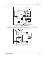
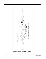
The digital input buffer circuits shown in Figures 15 and 16 accept and drive industry standard
RS-422, RS-423, and RS-232 signal levels. These circuits may be used to convert from one signal
format to another.
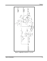
The digital output circuit shown in Figure 15 can be conÞgured by the user to provide SONY
CCU compatible I/O; contact closure circuits are not provided on connectors 2, 4, 6, and 8. Refer
to Table 4, ÒDigital Cable Connections,Ó on page 7 for instructions on selecting the CCU
capability. When this option is selected, the RS-422 and RS-232 serial communications for that
connector are not available.
The circuits in Figure 15 also provide contact closure inputs and outputs. The contact closure
inputs are made by connecting pin 8 to ground (pin 3). This may be accomplished with a TTL
output referenced to pin 3 as ground. The output contact closure is an SPST-NO relay and is not
ground referenced.

