© Teledyne UK Limited 2020
Document subject to disclaimer on page 1
A1A-795787 Version 1, page 11
DEEP DEPLETED AIMO DEVICE TECHNOLOGY
Extending the long wavelength response of back-face devices requires the use of thicker silicon, but this
must be fully depleted to avoid loss of spatial resolution through sideways diffusion of charge. The depth of
depletion is proportional to square root of the operating voltages and the silicon resistivity, but there is a
practical limit to both and possibilities for maintaining full-depletion with increasing thickness are therefore
limited.
In standard devices the bulk of the silicon substrate is all at the same bias voltage V
SS
. It is possible to take
V
SS
to negative voltages to increase depletion, but the limit is generally set by the onset of avalanche
breakdown in the p-n junctions of the output circuit components. For AIMO devices the high positive
substrate voltage required to achieve surface potential pinning and reduce dark signal further reduces the
achievable depletion depth.
The use of a lower or negative substrate bias on the back of the silicon V
BSS
to increase the depth of
depletion under the electrodes, whilst still maintaining a bias on the front-surface of the silicon V
FSS
at a
voltage level normally used for V
SS
allows the output circuits to function normally and pinning to be
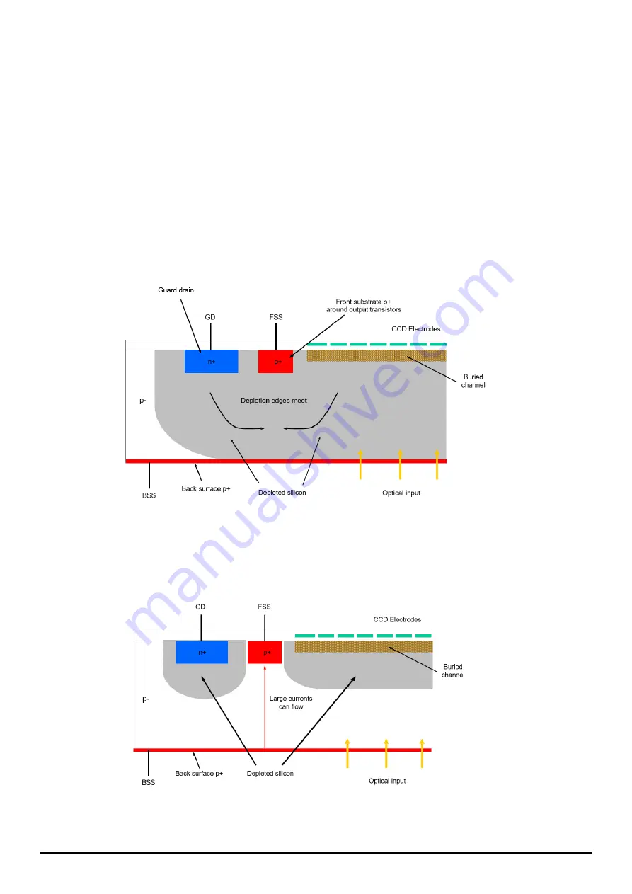
maintained. However, for this to be possible, current flow between the front and back bias connections must
be avoided. This is achieved using an additional “guard drain” diode at bias V
GD
, as shown below.
With correct bias conditions the depletion regions from the CCD channel and the guard diode merge to block
the conductive path, rather like the operation of a JFET, as shown above. If incorrect, then there is a direct
resistive path between the front and back contacts and excessive currents can flow, as shown below.
It is therefore important to use the specified bias levels and the switch-on and switch-off sequences.


