S50 Hardware User Guide
1VV0301505 Rev. 3
Page 25 of 60
2021-05-05
Not Subject to NDA
4.11.
Analog/Digital Converter (ADC)
Functionality is defined project specific in the firmware used.
The ADC supports:
•
8/10/12-bit resolution, 14-bit resolution with oversampling
•
Full swing operation 0V to VSUP
•
Up to 200kHz sample rate
•
Limit event monitoring
•
2 sources for ADC reference voltage 600mV REF or VSUP/4
•
Prescaler [1/6, 1/5, 1/4, 1/3, 1/2, 1, 2, 4]
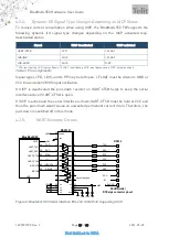
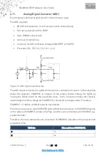
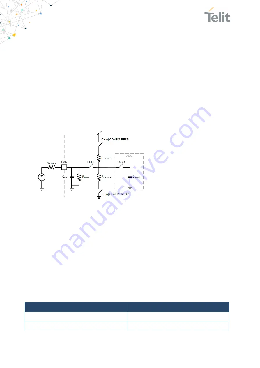
Figure 15: ADC Signal Input Structure
The ADC signal conversion is splitted into 2 phases, sample and convert. In the sampling
phase the capacitor CSAMPLE is charges to the analog source voltage for tACQ, by
closing the TACQ switch for the acquisition time. In the conversion phase the TACQ is
opened again and the voltage on CSAMPLE is converted to a digital value. Therefore,
FSAMPLE < 1/ (tACQ + tCONV) must be maintained.
The time necessary to load CSAMPLE with sufficient preciseness to VSOURCE depends
on the values of CSAMPLE, known 2,5pF typ., and the source resistance of VSOURCE, e.g.
a potentiometer.
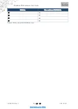
Therefore, the max. allowed source resistance of VSOURCE depends on the programmed
acquisition time.
TACQ /µs
Max. resistance VSOURCE /k
Ω
3
10
5
40

