S50 Hardware User Guide
1VV0301505 Rev. 3
Page 40 of 60
2021-05-05
Not Subject to NDA
7.5.
OEM Layout and Antenna Selection in Respect to
RED/FCC/IC Certification
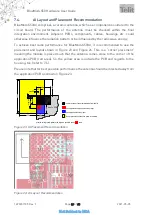
Placement for S50/AP, is not restricted. For antenna port connection it is
recommended to use a layout like shown in Figure 26.
To keep specified radio power values the impedance of the RF trace connected to the
antenna port shall be 50 Ohms. Impedance of the RF trace depends on customer pcb. Use
a calculator for coplanar waveguides e.g. “TXline” to determine track width and gap
between ground and RF track.
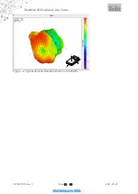
Figure 25: Coplanar Waveguide Sample
Figure 26: AP Antenna Port Layout Recommendation
OEM integrators are free with choosing a trace design suitable for their end product and
selecting an antenna according to their needs. Only if it is desired to re-use the RED/FCC
and IC certification of the S50/AP the following restrictions apply.
1.
Use External Antenna: antenova part no B4844-R
Please note that for FCC Certification it is mandatory to use a reverse SMA
connector instead of using a standard SMA male connector on the antenna side.
2.
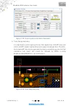
Exactly follow the Trace Design with below given parameters
The RF trace on the Telit standalone test board used for homologation lab testing
is placed on the top side of a standard FR4 4 layer PCB with
ε
r
≈
4,7 and designed
as microstrip transmission line with the below given parameters.
In many cases the antenna is required to be mounted in another position on the
end product. This could be achieved by using SMA/SMA coax cables.
a.
Trace Design Impedance 50R Calculation

