background image


GE864-QUAD Automotive V2 Hardware User Guide 

1vv0300840 Rev.0.1  24/11/09    


Reproduction forbidden without Telit Communications S.p.A. written authorization - All Rights Reserved 


page 57 of 65 


11.3.4 Debug of the GE864 in production 

 
To test and debug the mounting of the GE864, we strongly recommend to foreseen test pads on the 
host PCB, in order to check the connection between the GE864 itself and the application and to test 
the performance of the module connecting it with an external computer. Depending by the customer 
application, these pads include, but are not limited to the following signals: 

 TXD 

 RXD 

 ON/OFF 

 RESET 

 GND 

 VBATT 

 TX_TRACE 

 RX_TRACE 


PWRMON 


11.3.5 Stencil 

 
Stencil’s apertures layout can be the same of the recommended footprint (1:1), we suggest a 
thickness of stencil foil 

 120µm. 

Summary of Contents for GE864-QUAD Automotive V2

Page 1: ...GE864 QUAD Automotive V2 Hardware User Guide 1vv0300840 Rev 0 1 24 11 09...

Page 2: ...re User Guide 1vv0300840 Rev 0 1 24 11 09 Reproduction forbidden without Telit Communications S p A written authorization All Rights Reserved page 2 of 65 This document is relating to the following pr...

Page 3: ...ly 20 5 1 Power Supply Requirements 20 5 2 Power Consumption 21 5 3 General Design Rules 22 5 3 1 Electrical Design Guidelines 22 5 3 1 1 5V input Source Power Supply Design Guidelines 22 5 3 1 2 12V...

Page 4: ...cation of network service availability 50 10 9 RTC Bypass out 51 10 10 External SIM Holder Implementation 51 11 DAC and ADC section 52 11 1 DAC Converter 52 11 1 1 Description 52 11 1 2 Enabling DAC 5...

Page 5: ...anding the foregoing Telit does not make any warranty as to the information contained herein and does not accept any liability for any injury loss or damage of any kind incurred by use of or reliance...

Page 6: ...UAD Automotive V2 cellular module within user application shall be done according to the design rules described in this manual IT L integrazione del modulo cellulare GSM GPRS GE864 QUAD Automotive V2...

Page 7: ...09 Reproduction forbidden without Telit Communications S p A written authorization All Rights Reserved page 7 of 65 2 GE864 QUAD Automotive V2 Mechanical Dimensions The Telit GE864 QUAD Automotive V2...

Page 8: ...andsfree ear output phase Audio SIM card interface C10 SIMCLK O External SIM signal Clock 1 8 3V C11 SIMIN I External SIM signal Presence active low 47K 1 8 3V D4 SIMVCC External SIM signal Power supp...

Page 9: ...it GPIO01 I O pin Jammer detect report CMOS 2 8V H5 GPIO_02 PCM_WAO I O Telit GPIO02 Configurable GPIO PCM audio CMOS 2 8V K7 GPIO_03 PCM_RX I O Telit GPIO03 Configurable GPIO PCM audio CMOS 2 8V B3 G...

Page 10: ...GND Ground Power RESERVED A3 Reserved A4 Reserved A5 Reserved A6 Reserved A7 Reserved A8 Reserved A9 Reserved A10 Reserved B1 Reserved B2 Reserved B4 Reserved B8 Reserved B9 Reserved B10 Reserved B11...

Page 11: ...eserved H4 Reserved H6 Reserved H7 Reserved J4 Reserved J6 Reserved J7 Reserved K9 Reserved K10 Reserved K11 Reserved L5 Reserved L7 Reserved L10 Reserved Ref to Digital Voice Interface Application No...

Page 12: ...2 RESET VRTC GND VBATT VBATT GND 3 GPIO_04 32K_IN GPIO_08 PCM_TX GND GND GND 4 SIMVCC GND Antenna 5 GPIO_06 ALARM GPIO_02 PCM_WAO ON_OFF GND 6 C125 RING GND GPIO_01 JDR C106 CTS GND GND 7 C108 DTR DAC...

Page 13: ...ommunications S p A written authorization All Rights Reserved page 13 of 65 AUDIO Signals balls SIM CARD interface balls TRACE Signals balls Prog data Hw Flow Control signals balls ADC signals balls M...

Page 14: ...A simple circuit to do it is NOTE don t use any pull up resistor on the ON line it is internally pulled up Using pull up resistor may bring to latch up problems on the GE864 QUAD Automotive V2 power r...

Page 15: ...dware User Guide 1vv0300840 Rev 0 1 24 11 09 Reproduction forbidden without Telit Communications S p A written authorization All Rights Reserved page 15 of 65 A flow chart showing the proper turn on p...

Page 16: ...Telit Communications S p A written authorization All Rights Reserved page 16 of 65 For example 1 Let s assume you need to drive the ON pad with a totem pole output from 1 8V up to 5V microcontroller...

Page 17: ...conditional Restart When the device is shut down by software command or by hardware shutdown it issues to the network a detach request that informs the network that the device will not be reachable an...

Page 18: ...orization All Rights Reserved page 18 of 65 4 2 2 Hardware Unconditional Restart To unconditionally Restart the GE864 QUAD Automotive V2 the pad RESET must be tied low for at least 200 milliseconds an...

Page 19: ...n the GE864 QUAD Automotive V2 power regulator and improper functioning of the module The line RESET must be connected only in open collector configuration TIP The unconditional hardware Restart shoul...

Page 20: ...ts and the guidelines that will follow for a proper design 5 1 Power Supply Requirements POWER SUPPLY Nominal Supply Voltage 3 8V Max Supply Voltage 4 2V Operating Supply Voltage Range 3 4V 4 2V Wide...

Page 21: ...g data mode GSM TX and RX mode Min power level 78 1 Max power level 200 1 GSM Sending data mode GPRS class 10 TX and RX mode Min power level 123 7 Max power level 370 8 GPRS Sending data mode The GSM...

Page 22: ...5V input Source Power Supply Design Guidelines The desired output for the power supply is 3 8V hence there s not a big difference between the input source and the desired output and a linear regulato...

Page 23: ...lows the regulator to respond quickly to the current peaks absorption In any case the frequency and Switching design selection is related to the application to be developed due to the fact the switchi...

Page 24: ...de 1vv0300840 Rev 0 1 24 11 09 Reproduction forbidden without Telit Communications S p A written authorization All Rights Reserved page 24 of 65 An example of switching regulator with 12V input is in...

Page 25: ...ve V2 and damage it NOTE DON T USE any Ni Cd Ni MH and Pb battery types directly connected with GE864 QUAD Automotive V2 Their use can lead to overvoltage on the GE864 QUAD Automotive V2 and damage it...

Page 26: ...nificantly only during calls If we assume that the device stays into transmission for short periods of time let s say few minutes and then remains for a quite long time in idle let s say one hour then...

Page 27: ...at the current peaks frequency of 216 Hz that will reflect on all the components connected to that supply introducing the noise floor at the burst base frequency For this reason while a voltage drop...

Page 28: ...ng requirements ANTENNA REQUIREMENTS Frequency range Depending by frequency band s provided by the network operator the customer shall use the most suitable antenna for that those band s Bandwidth 70...

Page 29: ...Bi 900 3dBi 1800 1 4dBi 850 and 3dBi 1900 gain for mobile and fixed operating configurations 6 2 GSM Antenna PCB line Guidelines Ensure that the antenna line impedance is 50 ohm Keep the antenna line...

Page 30: ...na Installation Guidelines Install the antenna in a place covered by the GSM signal The Antenna must be installed to provide a separation distance of at least 20 cm from all persons and must not be co...

Page 31: ...Automotive V2 interface circuits Absolute Maximum Ratings Parameter Min Max Input level on any digital pin when on 0 3V 3 1V Input voltage on analog pins when on 0 3V 3 0 V Operating Range Interface l...

Page 32: ...set signal must not be used to normally shutting down the device but only as an emergency exit in the rare case the device remains stuck waiting for some network response The RESET is internally contr...

Page 33: ...roller UART 5V or other voltages different from 2 8V Depending from the type of serial port on the OEM hardware a level translator circuit may be needed to make the system work The only configuration...

Page 34: ...H1 L1 H2 L2 J3 K3 Ground ground 6 DSR dsr_uart E11 Data Set Ready Output from the GE864 QUAD Automotive V2 that indicates the module is ready 7 RTS rts_uart F7 Request to Send Input to the GE864 QUAD...

Page 35: ...nslator not a RS485 or other standards By convention the driver is the level translator from the 0 3V UART level to the RS232 level while the receiver is the translator from RS232 level to 0 3V UART I...

Page 36: ...6 of 65 An example of level translation circuitry of this kind is The example is done with a SIPEX SP3282EB RS232 Transceiver that could accept supply voltages lower than 3V DC In this case Vin has to...

Page 37: ...case the compliance with RS232 5V is possible Another level adapting method could be done using a standard RS232 Transceiver MAX3237EAI adding some resistors to adapt the levels on the GE865 Input li...

Page 38: ...2 8 3V then a circuitry has to be provided to adapt the different levels of the two set of signals As for the RS232 translation there are a multitude of single chip translators For example a possible...

Page 39: ...V2 input lines connected to open collector outputs in order to avoid latch up problems on the GE864 QUAD Automotive V2 Care must be taken to avoid latch up on the GE864 QUAD Automotive V2 and the use...

Page 40: ...set function HF lines is suited for hands free function car kit These two blocks can be active only one at a time selectable by AXE hardware line or by AT command The audio characteristics are equival...

Page 41: ...hands free function car kit TIP being the microphone circuitry the more noise sensitive its design and layout must be done with particular care Both microphone paths are balanced and the OEM circuitr...

Page 42: ...mVrms Microphone nominal sensitivity 45 dBVrms Pa Analog gain suggested 20dB Echo canceller type Handset MIC_HF 2nd differential microphone path Line Coupling AC Line Type Balanced Coupling capacitor...

Page 43: ...ive an external amplifier or directly a 16 earpiece at 12dBFS the EAR_HF lines EPPA1_2 and EPPA2 are the Fully Differential Power Buffers they can directly drive a 16 speaker in differential balanced...

Page 44: ...l bandwidth 150 4000 Hz 3 dB Differential output voltage 328mVrms 16 12dBFS SW volume level step 2 dB Number of SW volume steps 10 EAR_HF Power Buffers Path Line Coupling DC Line Type Bridged Output l...

Page 45: ...Configurable GPIO CMOS 2 8V 1uA 1mA INPUT HIGH see Fig 01 Alternate function ALARM E6 GPIO_01 I O GPIO01 Configurable GPIO CMOS 2 8V 1uA 1mA INPUT x Alternate function JDR H3 GPIO_08 I O GPIO08 Confi...

Page 46: ...ications used in the GE864 QUAD Automotive V2 interface circuits Absolute Maximum Ratings Parameter Min Max Input level on any digital pin when on 0 3V 3 1V Input voltage on analog pins when on 0 3V 3...

Page 47: ...be connected with the GPIO input pad has interface levels different from the 2 8V CMOS then it can be buffered with an open collector transistor with a 47K pull up to 2 8V 10 3 Using a GPIO Pad as OU...

Page 48: ...Alarm Output is controlled by the GE864 QUAD Automotive V2 module and will rise when the alarm starts and fall after the issue of a dedicated AT command This output can be used to power up the GE864...

Page 49: ...cations S p A written authorization All Rights Reserved page 49 of 65 A sample interface scheme is included below to give you an idea of how to interface a Buzzer to the GPIO7 NOTE To correctly drive...

Page 50: ...on the network service availability and Call status In the GE864 QUAD Automotive V2 modules the STAT_LED usually needs an external transistor to drive an external LED Therefore the status indicated i...

Page 51: ...al Time Clock supply which is separate from the rest of the digital part allowing having only RTC going on when all the other parts of the device are off To this power output a backup capacitor can be...

Page 52: ...omotive V2 module and on pin 17 of PL102 on EVK2 Board CS1302 The on board DAC is a 10 bit converter able to generate a analogue value based a specific input in the range from 0 up to 1023 However an...

Page 53: ...T command is available to use the DAC function The command is AT DAC enable value value scale factor of the integrated output voltage 0 1023 10 bit precision it must be present if enable 1 Refer to SW...

Page 54: ...convert it into 11 bit word Min Max Units Input Voltage range 0 1 9 Volt AD conversion 11 bits Resolution 1 mV The GE864 QUAD Automotive V2 module provides 2 Analog to Digital Converters The input lin...

Page 55: ...rization All Rights Reserved page 55 of 65 11 3 Mounting the GE864 QUAD Automotive V2 on your Board 11 3 1 General The Telit GE864 QUAD Automotive V2 modules have been designed in order to be complian...

Page 56: ...ardware User Guide 1vv0300840 Rev 0 1 24 11 09 Reproduction forbidden without Telit Communications S p A written authorization All Rights Reserved page 56 of 65 11 3 3 Recommended foot print for the a...

Page 57: ...to foreseen test pads on the host PCB in order to check the connection between the GE864 itself and the application and to test the performance of the module connecting it with an external computer D...

Page 58: ...Communications S p A written authorization All Rights Reserved page 58 of 65 11 3 6 PCB pad design Non solder mask defined NSMD type is recommended for the solder pads on the PCB Recommendations for...

Page 59: ...e Holes in pad are allowed only for blind holes and not for through holes Recommendations for PCB pad surfaces Finish Layer thickness m Properties Electro less Ni Immersion Au 3 7 0 05 0 15 good solde...

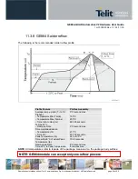
Page 60: ...min Temperature Max Tsmax Time min to max ts 150 C 200 C 60 180 seconds Tsmax to TL Ramp up Rate 3 C second max Time maintained above Temperature TL Time tL 217 C 60 150 seconds Peak Temperature Tp 24...

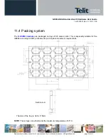
Page 61: ...ization All Rights Reserved page 61 of 65 11 4 Packing system The Telit GE864 modules are packaged on trays of 20 pieces each This is especially suitable for the GE864 according to SMT processes for p...

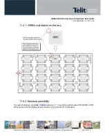
Page 62: ...unications S p A written authorization All Rights Reserved page 62 of 65 11 4 1 GE864 orientation on the tray 11 4 2 Moisture sensibility The level of moisture sensibility of GE864 module is 3 in acco...

Page 63: ...the essential requisite of the R TTE 99 5 EC directive the GE864 QUAD Automotive V2 module is compliant with the following standards GSM Radio Spectrum Standard EN 301 511 and 3GPP 51 010 1 EMC Electr...

Page 64: ...ons have to be taken for the SIM checking carefully the instruction for its use Do not insert or remove the SIM when the product is in power saving mode The system integrator is responsible of the fun...

Page 65: ...without Telit Communications S p A written authorization All Rights Reserved page 65 of 65 14 Document Change Log R Re ev vi is si io on n D Da at te e C Ch ha an ng ge es s ISSUE 0 01 07 08 First Rel...

Reviews: