


GL865 Hardware User Guide
1vv0300910 Rev.1 – 2011-07-22
Reproduction forbidden without Telit Communications S.p.A. written authorization - All Rights Reserved
page 33 of 79
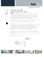
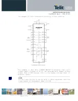
Coupling with other signals shall be
avoided
Cold End (Ground Plane) of antenna shall be
equipotential to the GL865 ground pins
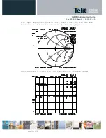
7.2.
GSM Antenna - PCB line Guidelines
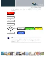
Make sure that the transmission line’s characteristic impedance
is 50
Ω
;
Keep the length of line on the PCB as short as possible, since
the antenna line loss shall be less than about 0,3 dB;
Line geometry should have uniform characteristics, constant
cross section, avoid meanders and abrupt curves;
Any kind of suitable geometry / structure (Microstrip, Stripline,
Coplanar, Grounded Coplanar Waveguide...) can be used for
implementing the printed transmission line afferent the antenna;
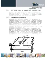
If a Ground plane is required in line geometry, that plane has
to be continuous and sufficiently extended, so the geometry can
be as similar as possible to the related canonical model;
Keep, if possible, at least one layer of the PCB used only for
the Ground plane. If possible, use this layer as reference
Ground plane for the transmission line;
It is wise to surround (on both sides) the PCB transmission line
with Ground, avoid having other signal tracks facing directly
the antenna line track.
Avoid crossing any un-shielded transmission line footprint with
other signal tracks on different layers;
The ground surrounding the antenna line on PCB has to be
strictly connected to the main Ground Plane by means of via
holes (once per 2mm at least), placed close to the ground edges
facing line track;
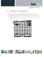
Place EM noisy devices as far as possible from GL865 antenna
line;
Keep the antenna line far away from the GL865 power supply
lines;
If EM noisy devices are present on the PCB hosting the GL865,
such as fast switching ICs, take care of the shielding of the
antenna line by burying it inside the layers of PCB and surround
it with Ground planes, or shield it with a metal frame cover.
If EM noisy devices are not present around the line, the use of
geometries like Microstrip or Grounded Coplanar Waveguide has to
be preferred, since they typically ensure less attenuation if
compared to a Stripline having same length;


