


GL865 Hardware User Guide
1vv0300910 Rev.1 – 2011-07-22
Reproduction forbidden without Telit Communications S.p.A. written authorization - All Rights Reserved
page 55 of 79
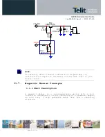
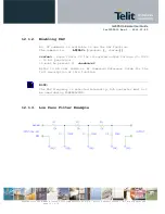
11.
General Purpose I/O
The general purpose I/O pads can be configured to act in three
different ways:
•
input
•
output
•
alternate function (
internally controlled
)
Input pads can only be read; they report the digital value (
high
or low
) present on the pad at the read time .
Output pads can only be written or queried and set the value of
the pad output.
An alternate function pad is internally controlled by the GL865
firmware and acts depending on the function implemented.
For Logic levels please refer to chapter 8.
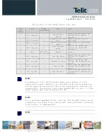
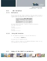
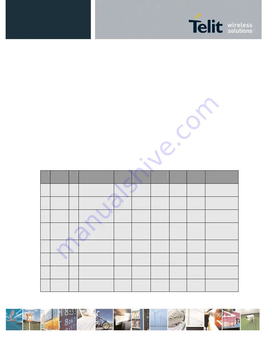
The following table shows the available GPIO on the GL865.
Pin Signal I/O
Function
Type
Input /
output
current
Default
State
ON_OFF
state
State
during
Reset
Note
42 GPIO_01 I/O
Configurable
GPIO
CMOS
2.8V
1uA/1mA
INPUT
0
0
Alternate
function
DVI_WA0
41 GPIO_02 I/O
Configurable
GPIO
CMOS
2.8V
1uA/1mA
INPUT
0
0
Alternate
function JDR
and DVI_RX
40 GPIO_03 I/O
Configurable
GPIO
CMOS
2.8V
1uA/1mA
INPUT
0
0
Alternate
function
DVI_TX
39 GPIO_04 I/O
Configurable
GPIO
CMOS
2.8V
1uA/1mA
INPUT
0
0
Alternate
function TX
disable and
DVI_CLK
29 GPIO_05 I/O
Configurable
GPIO
CMOS
2.8V
1uA/1mA
INPUT
0
0
Alternate
function
RFTXMON
28 GPIO_06 I/O
Configurable
GPIO
CMOS
2.8V
1uA/1mA
INPUT
0
0
Alternate
function
ALARM
27 GPIO_07 I/O
Configurable
GPIO
CMOS
2.8V
1uA/1mA
INPUT
0
0
Alternate
function
BUZZER
26 GPIO_08 I/O
Configurable
GPIO
CMOS
2.8V
1uA/1mA
INPUT
0
0
Alternate
function
STAT_LED


