

WE865-DUAL HW User Guide
1vv0300787
Rev. 1 - 03/10/08
Reproduction forbidden without Telit Communications S.p.A. written authorization - All Rights Reserved
page 41 of 48
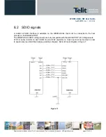
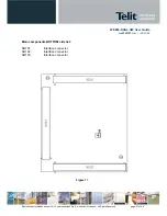
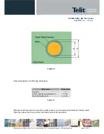
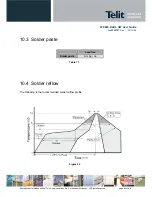
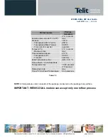
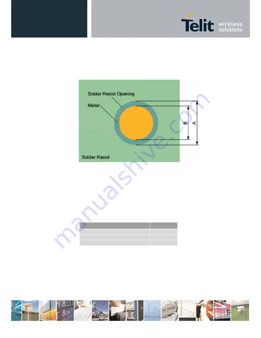
Figure 20
Recommendations for PCB pad dimensions
Dimension
Value [mm]
Ball pitch
2
Solder resist opening diameter A
1,150
Metal PAD diameter B
1 +/- 0,05
Table 15
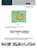
Placement of microvias not covered by solder resist is not recommended inside the “Solder resist
Opening”,unless the microvia carry the same signal of the pad itself.