WE865-DUAL HW User Guide
1vv0300787
Rev. 1 - 03/10/08
Reproduction forbidden without Telit Communications S.p.A. written authorization - All Rights Reserved
page 42 of 48
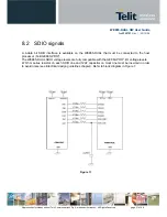
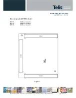
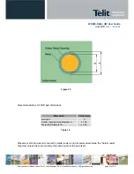
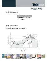
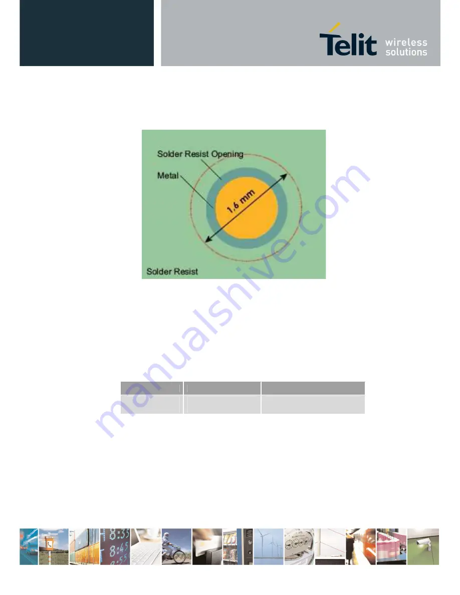
Figure 21
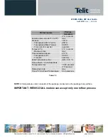
Holes in pad are allowed only for blind holes and not for through holes.
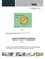
Recommendations for PCB pad surfaces:
Finish
Layer tickness [um]
Properties
Electro-less Ni /
Immersion Au
3-7 /
0,05-0,15
good solder ability protection,
high shear force values
Table 16
The PCB must be able to resist the higher temperatures, which are occurring at the lead-free process.
This issue should be discussed with the PCB-supplier. Generally, the wet-ability of tin-lead solder
paste on the described surface plating is better compared to lead-free solder paste.