xE70-915 RF Module User Guide
1VV0301106
rev.3 – 2015-03-04
Reproduction forbidden without written authorization from Telit Communications S.p.A. - All Rights
Reserved.
Page 20 of 34
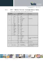
4.4.
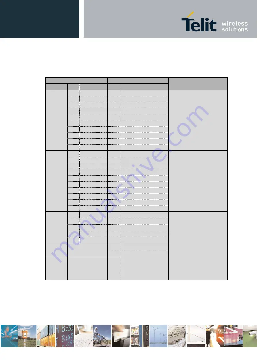
DIP – Module Pin-out Correspondence Table
Pin-Out correspondence between xE70-915/DIP and xE70-915/SMD
xE70-915/DIP
xE70-915/SMD
Comments
Connector Pin
Name
Pin
Name
J1
1
2
GND
GND
3
P1
J5
IO5_A
4
P2
J9
Status TX/RX
Reserved Pin
5
P3
J2
RX LED
6
P4
J1
TX LED
7
P5
J4
IO4_A
8
P6
J3
IO3_A
9
GND
GND
10
VDD
J25
VDD
J2
11
PROG
J16
PROG
12
RTS
J22
RTS
13
CTS
J24
CTS
14
RESET
J23
RESET
15
RxD
J21
RxD
16
TxD
J19
TxD
17
STDBY
J18
STAND_BY
18
RTS
J22
RTS
19
P7
J6
IO6_A
20
GND
GND
J4
1
J14
PDI_DATA
J4 Connector for debugging and
flashing
2
J10
PDI_CLK
3
J23
RESET
4
J25
VDD
5
GND
J7
IO7_A
Reserved Pin
J8
IO8_AD_DA
J3
SMA connector
J29
Ext_Antenna
(Unbalanced RF)
A 50 Ohm coplanar wave guide
and a 0 ohm resistor are used to
connect J29 to J3


