xE70-915 RF Module User Guide
1VV0301106
rev.3 – 2015-03-04
Reproduction forbidden without written authorization from Telit Communications S.p.A. - All Rights
Reserved.
Page 27 of 34
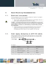
6.3.
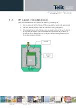
RF layout considerations
Basic recommendations must be followed to achieve a good RF layout:
•
It is recommended to fill all unused PCB area around the module with ground plane
•
The radio module ground pin must be connected to solid ground plane.
•
If the ground plane is on the bottom side, a via (metal hole) must be used in front of
each ground pad. Especially J28 and J30 (RF Gnd) pins should be grounded via
several holes to be located right next to the pins, thus minimizing inductance and
preventing mismatch and losses.


