11
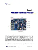
PSoC Development Kit or CY8CKIT-030 PSoC 3 Development Kit. The header carries voltage
enables, regulator voltage, regulator load currents and trim/margin control signals for each regulator
on PME EBK. The I2C physical layer signals (SDA/SCL) from PSoC are also routed across this
header to enable connection to an external host or management processor that supports standard I2C,
SMBus or PMBus protocol interfaces.
3.1
2x20 pin Interface Header
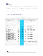
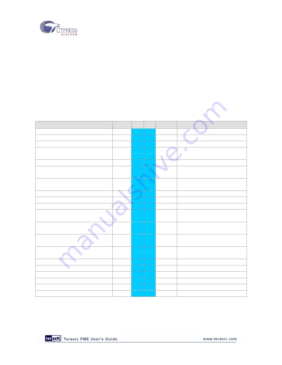
The following table outlines the definition of the 40-pin J1 header interface.
Table 3-1 2x20 Header (J1) Pin Definition
Description
Signal
Pin
Pin
Signal
Description
Voltage Regulator 4, Enable
V4EN
1
2
V3EN
Voltage Regulator 3, Enable
Voltage Regulator 2, Enable
V2EN
3
4
V1EN
Voltage Regulator 1, Enable
- NC
5
6 NC -
Power Rail Current
(measured as single ended voltage)
IIN
7
8
VIN
Power Rail Sensing Voltage
Analog Ground
AGND
9
10
NC -
Voltage Regulator 4, Fault Sensing
Voltage
C4
11
12
C3
Voltage Regulator 3, Fault
Sensing Voltage
Voltage Regulator 2, Fault Sensing
Voltage
C2
13
14
C1
Voltage Regulator 1, Fault
Sensing Voltage
Voltage Regulator 4, Trim
TR4
15
16
TR3 Voltage
Regulator
3,
Trim
Voltage Regulator 2, Trim
TR2
17
18
TR1 Voltage
Regulator
1,
Trim
Analog Ground
AGND
19
20
NC -
Voltage Regulator 4, Current
(Measured as differential voltage)
I4
21
22
V4 Voltage
Regulator
4
Voltage Regulator 3, Current
(Measured as differential voltage)
I3
23
24
V3 Voltage
Regulator
3
Voltage Regulator 2, Current
(Measured as differential voltage)
I2
25
26
V2 Voltage
Regulator
2
Voltage Regulator 1 Current
(Measured as single ended voltage)
I1
27
28
V1 Voltage
Regulator
1
Analog Ground
AGND
29
30
NC -
- NC
31
32
/ALERT
Alert Signal (I2C/SMBus/PMBus)
Serial Data (I2C/SMBus/PMBus)
SDAT
33
34
SCL
Serial Clock (I2C/SMBus/PMBus)
unused
D3V3
35
36
VADJ
unused
Digital Ground
DGND
37
38
D5V
unused
Optional 12V Power from DVK
DVIN
39
40
DGND Digital
Ground
Summary of Contents for CY8CKIT-035
Page 1: ......
Page 38: ...Chapter 5 Schematics 5 1 Primary 12V Power Input 37 ...
Page 39: ...5 2 DVK Connector and Debug Test Points 5 3 Voltage Regulator V1 5V 38 ...
Page 40: ...5 4 Voltage Regulator V2 3 3V 5 5 Voltage Regulator V3 2 5V 5 6 Voltage Regulator V4 1 8V 39 ...
Page 41: ...5 7 I2C SMBus PMBus Interface Connector 5 8 Layout 5 8 1 Top Layer 40 ...
Page 42: ...5 8 2 Ground Layer 5 8 3 Power Layer 41 ...
Page 43: ...5 8 4 Bottom Layer 42 ...
Page 44: ...5 8 5 Top Silkscreen 43 ...


