Technical Details – Voltage Sequencing
This example builds upon the
Voltage Sequencer
component discussed in Cypress Application Note
AN62496
“Voltage Sequencing with PSoC
®
3 and PSoC
®
5”. The
Voltage Sequencer
component
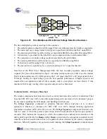
enables designers to control both the power-up and power-down sequence and timing of up to 16
secondary-side voltage supplies. It is designed to interface to regulators that provide a digital power
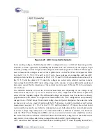
good (PGOOD) status output. In this example project, the regulators on the PSoC Power
Management EBK are monitored using the under-voltage/over-voltage window comparator logic
inside PSoC with programmable thresholds on each rail which generate equivalent PGOOD signals
internally that connect to the
Voltage Sequencer
component. (See
Figure 4-12
)
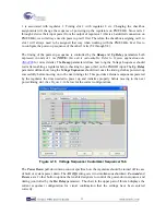
Figure 4-12 Advanced Sequencer Architecture
To change the behavior of the sequencer, double click on the
Voltage Sequencer
in the Example1
top-level design schematic file. (See
Figure 4-13
)
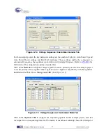
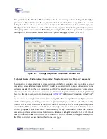
Figure 4-13 Voltage Sequencer Component
This will open the component customizer for the
Voltage Sequencer
. The
General Tab
will be
presented first by default. (See
Figure 4-14
)
21
Summary of Contents for CY8CKIT-035
Page 1: ......
Page 38: ...Chapter 5 Schematics 5 1 Primary 12V Power Input 37 ...
Page 39: ...5 2 DVK Connector and Debug Test Points 5 3 Voltage Regulator V1 5V 38 ...
Page 40: ...5 4 Voltage Regulator V2 3 3V 5 5 Voltage Regulator V3 2 5V 5 6 Voltage Regulator V4 1 8V 39 ...
Page 41: ...5 7 I2C SMBus PMBus Interface Connector 5 8 Layout 5 8 1 Top Layer 40 ...
Page 42: ...5 8 2 Ground Layer 5 8 3 Power Layer 41 ...
Page 43: ...5 8 4 Bottom Layer 42 ...
Page 44: ...5 8 5 Top Silkscreen 43 ...


