29
When the trimming menu is displayed, pressing and holding SW1 on the CY8CKIT-001 PSoC
DVK (SW2 on the CY8CKIT-030 PSoC 3 DVK) for a longer period will enable manual trimming
control for the next secondary regulator. To get back to the main voltage display menu, cycle
through all 4 manual trim menus by pressing and holding SW1 on the CY8CKIT-001 PSoC DVK
(SW2 on the CY8CKIT-030 PSoC 3 DVK) for a longer period.
Technical Details – Voltage Sequencer and Under/Over-Voltage Fault Detection
The voltage sequencer and under/over-voltage window comparator circuits are fundamentally the
same in this example as they were for Example1, so they will not be discussed again here.
One thing to note is that when running the example project on the CY8CKIT-030 PSoC 3 DVK,
only 2 of the voltage rails (V1=5V and V3=2.5V) can be routed to the window comparator circuit
due to the PSoC port pins available on Port E of the DVK. The other voltage rails (V2=3.3V and
V4=1.8V) are monitored using the ADC and compared against the under/over voltage thresholds
using a +/-10% window. When running this example project on the CY8CKIT-030 PSoC 3 DVK, it
may not be possible to generate faults on those rails using the switches in the trimming menus.
Technical Details – Voltage and Current Measurements
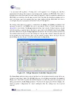
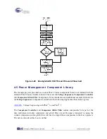
In Example2, voltage rail voltage and current measurements use the differential 12-bit Delta-Sigma
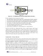
ADC with 0.1% internal accurate voltage reference. The PSoC Creator circuit is shown below:
(
Figure 4-23
)
Summary of Contents for CY8CKIT-035
Page 1: ......
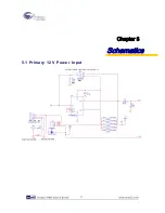
Page 38: ...Chapter 5 Schematics 5 1 Primary 12V Power Input 37 ...
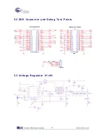
Page 39: ...5 2 DVK Connector and Debug Test Points 5 3 Voltage Regulator V1 5V 38 ...
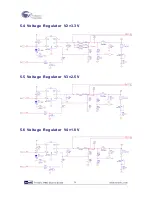
Page 40: ...5 4 Voltage Regulator V2 3 3V 5 5 Voltage Regulator V3 2 5V 5 6 Voltage Regulator V4 1 8V 39 ...
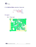
Page 41: ...5 7 I2C SMBus PMBus Interface Connector 5 8 Layout 5 8 1 Top Layer 40 ...
Page 42: ...5 8 2 Ground Layer 5 8 3 Power Layer 41 ...
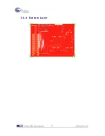
Page 43: ...5 8 4 Bottom Layer 42 ...
Page 44: ...5 8 5 Top Silkscreen 43 ...

