Application Note P4097
© TeraTron GmbH
Page 3 of 21
V1.1, 07.06.01
1. Introduction
This application note should give supplementary information about the integrated reader/exciter circuit
P4097.
The P4097 serves as interface between a transponder and a µController. The interface operates bi-
directional. The transponder is supplied with energy and data by on-off keying (OOK) of the carrier
signal and the transponder sends data back by modulating its quality factor (ASK/PSK).
The described circuit is a highly integrated solution for communicating with a transponder which is not
limited to a specific communication protocol and can read or write all kinds of transponder as long as
they use amplitude modulation. The amount of necessary external components is minimized.
Due to an integrated PLL there is no need for an external clock, the antenna circuit oscillates always
on its series resonance frequency. This, and the possibility to demodulate ASK and PSK signals
coming from the transponder, eliminate the “zero modulation” problem which occurs if the resonance
frequency of the transponder, the reader antenna and the driving frequency are mistuned by
component tolerances.
Furthermore the chip has been designed to support both, active and intelligent antenna. The
difference is the proximity of the controlling µC, either it sits close to the P4097 on the same PCB or it
is connected via a wiring harness where the number of wires is important and should be minimized.
Controlled by a serial interface the chip incorporates a power down mode as well as diagnostic
capabilities.
2. Function Principle
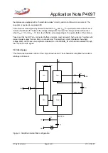
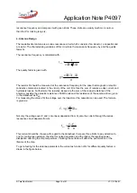
The interface between the transponder and the reader/exciter works like a transformer with very large
air gap and therefore a low coupling factor. The coupling factor can be visualized as ratio of the
received magnetic field by the transponder to the generated magnetic field by the reader/exciter. In
common applications this ratio is in the range of 0.5% to 5%.
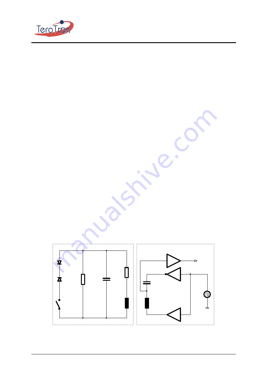
The transponder is energized by the received magnetic field and consumes little power which is
simulated by the resistor R
txp
. When sending data the transponder switches a voltage clipping element
in its resonant circuit which can be seen on the reader/exciter side as a small change of the voltage at
the antenna “tab” point (the voltage between the inductor L
ant
and the capacitor C
ant
referenced to
ground).
Rltxp
Driver
Reader/Exciter
Demodulator
Dmod2
Ltxp
GND
Smod
Lant
Transponder
Ctxp
Rtxp
Driver
to µC
Dmod1
Cant
Vant
Figure 1.: Transponder Interface equivalent circuit

