Application Note P4097
© TeraTron GmbH
Page 9 of 21
V1.1, 07.06.01
3.5 µC Interface
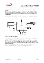
The inputs of the P4097 are IN, CLK and EC. All three pins are pulled down by a resistor with a typical
value of 50k
Ω
. The switching threshold is typical 50% of V
DD
. However, when using the worst case
values the connected µController should be able to source at least 140µA at V
DD
= 5V to achieve a
proper logic high level. This requires a R
DSon
of the p-channel FET (or a pull up) in the µController with
a value of less than 10.7k
Ω
.
The output OUT of the P4097 is a push-pull type with a worst case R
DSon
of about 500
Ω
. A typical
value at room temperature is between 150
Ω
and 200
Ω
.To achieve proper logic levels the load
resistance should be above 4.9k
Ω
. Due to the limited sink or source current the output is short circuit
protected against V
SS
and V
DD
.
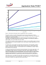
Care should be taken when the chip is not interfaced directly to a µController. The slew rate of the
clock signal should be high enough to achieve rise or fall times below 50ns. The chip is generating a
current spike during the polarity change of the 125kHz carrier signal (as any CMOS output) which can
crosstalk via ground into the clock signal. As the input does not incorporate any hysteresis only a
sufficient rise time guarantees that a clock pulse is not counted twice. Connected directly to a
µController the rise time should never cause a problem if a direct connection without additional filter
capacitors is chosen.
3.6 Active antenna interface
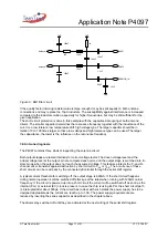
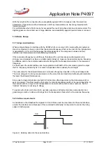
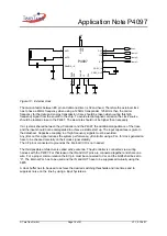
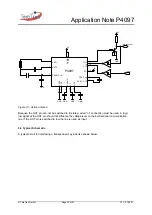
When the IN and OUT pin are connected together to form with the CLK signal a two wire interface this
configuration is called active antenna. It is advantageous if the antenna interface is a stand alone unit
without a µController. The wiring harness is then reduced to two supply wires plus two wires for the
digital interface.
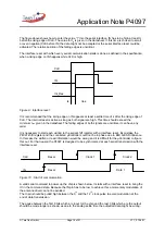
Because the OUT signal would modulate via the IN pin the antenna driver, both signals must be
decoupled via the data direction bit of the serial interface. This bit is enabled via the EC pin which is
not used if the P4097 is running with its own PLL and without an external clock.
The data direction bit is switching the interface between input and output. If in input mode the OUT pin
is pulled to ground. If in output mode the IN pin has no function but the antenna driver stays switched
on. This mode is left by an interface reset.
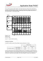
A simple transistor stage can form the interface to the wiring harness as shown in the chapter “modes
of operation” later in this application note.
3.7 Printed circuit board
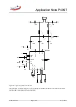
To achieve the maximum communication range the following design rules for the printed circuit board
should be regarded.
The V
SS
pin is the reference level for all analog signals. The antenna driver current which is sourced
out of the DV
SS
pin shall not have a common path with these analog signals.

