DS_1209F_004
73S1209F Data Sheet
Rev. 1.2
49
1.7.7 User (USR) Ports
The 73S1209F includes 9 pins of general purpose digital I/O (GPIO). On reset or power-up, all USR pins
are inputs until they are configured for the desired direction. The pins are configured and controlled by
the USR and UDIR
SFRs. Each pin declared as USR can be configured independently as an input or
output with the bits of the UDIRn
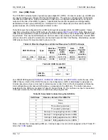
registers. Table 48 lists the direction registers and configurability
associated with each group of USR pins. USR pins 0 to 7 are multiple use pins that can be used for
general purpose I/O, external interrupts and timer control.
Table 49 shows the configuration for a USR pin through its associated bit in its UDIR register. Values
read from and written into the GPIO ports use the data registers
. Note: After reset, all
USR pins are defaulted as inputs and pulled up to VDD until any write to the corresponding UDIR register
is performed. This insures all USR pins are set to a known value until set by the firmware. Unused USR
pins can be set for output if unused and unconnected to prevent them from floating. Alternatively, unused
USR pins can be set for input and tied to ground or V
DD
.
Table 48: Direction Registers and Internal Resources for DIO Pin Groups
USR Pin Group
Type
Direction
Register
Name
Direction
Register
(SFR)
Location
Data
Register
Name
Data
Register
(SFR)
Location
USR_0…USR_7
Multi-use
UDIR70
0x91 [7:0]
USR70
0x90 [7:0]
USR_8
GPIO only
UDIR8
0xA1 [0]
USR8
0xA0 [0]
Table 49: UDIR Control Bit
UDIR Bit
0 1
USR Pin
Function
output input
Four XRAM SFR registers (
,
) control the use of the
USR [7:0] pins. Each of the USR [7:0] pins can be configured as GPIO or individually be assigned an
internal resource such as an interrupt or a timer/counter control. Each of the four registers contains two
3-bit configuration words named UxIS (where x corresponds to the USR pin). The control resources
selectable for the USR pins are listed in Table 74 through Table 78. If more than one input is connected
to the same resource, the resources are combined using a logical OR.
Table 50: Selectable Controls Using the UxIS Bits
UxIS Value
Resource Selected for USRx Pin
0 None
1 None
2
T0 (counter0 gate/clock)
3
T1 (counter1 gate/clock)
4
Interrupt 0 rising edge/high level on USRx
5
Interrupt 1 rising edge/high level on USRx
6
Interrupt 0 falling edge/low level on USRx
7
Interrupt 1 falling edge/low level on USRx
Note: x denotes the corresponding USR pin. Interrupt edge or level control is assigned in the IT0 and IT1
bits in the
register.


