


TPMC533 User Manual Issue 1.0.1
Page 75 of 107
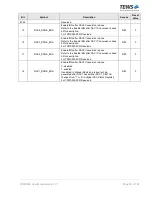
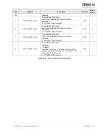
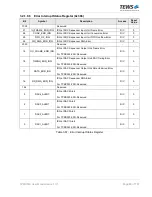
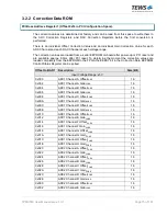
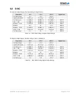
3.2.2 Correction Data ROM
PCI Base Address Register 1 (Offset 0x14 in PCI Configuration Space).
The correction values are determined at factory and can be read from this space to write them to
the ADC Correction Registers and DAC Correction Registers before the first conversion is
performed.
There is an individual Offset Correction Value and an individual Gain Correction Value for each
ADC Channel and each DAC Channel at each voltage range.
The correction values are loaded from a serial EEPROM on-board after power-up or PCI reset and
are available approx. 8.6ms after PCI reset. To determine the moment the correction values are
loaded completely from the EEPROM to the FPGA the EEBSY bit in the Correction Data EEPROM
Control/Status Register can be polled.
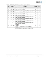
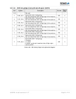
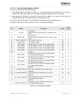
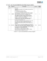
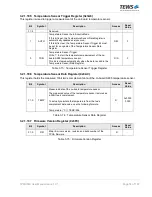
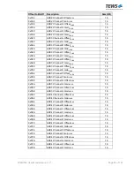
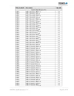
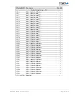
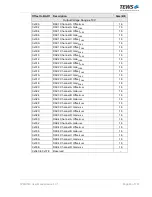
Offset to BAR1
Description
Size (Bit)
Input Voltage Range: ±5 V
0x000
ADC1 Channel A Offset
CORR
16
0x002
ADC1 Channel A Gain
CORR
16
0x004
ADC1 Channel B Offset
CORR
16
0x006
ADC1 Channel B Gain
CORR
16
0x008
ADC1 Channel C Offset
CORR
16
0x00A
ADC1 Channel C Gain
CORR
16
0x00C
ADC1 Channel D Offset
CORR
16
0x00E
ADC1 Channel D Gain
CORR
16
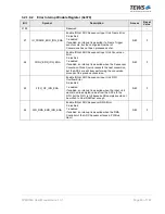
0x010
ADC1 Channel E Offset
CORR
16
0x012
ADC1 Channel E Gain
CORR
16
0x014
ADC1 Channel F Offset
CORR
16
0x016
ADC1 Channel F Gain
CORR
16
0x018
ADC1 Channel G Offset
CORR
16
0x01A
ADC1 Channel G Gain
CORR
16
0x01C
ADC1 Channel H Offset
CORR
16
0x01E
ADC1 Channel H Gain
CORR
16
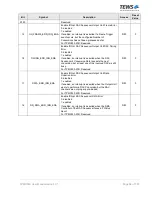
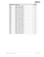
0x020
ADC2 Channel A Offset
CORR
16
0x022
ADC2 Channel A Gain
CORR
16
0x024
ADC2 Channel B Offset
CORR
16
0x026
ADC2 Channel B Gain
CORR
16
0x028
ADC2 Channel C Offset
CORR
16
0x02A
ADC2 Channel C Gain
CORR
16
0x02C
ADC2 Channel D Offset
CORR
16
0x02E
ADC2 Channel D Gain
CORR
16
0x030
ADC2 Channel E Offset
CORR
16
0x032
ADC2 Channel E Gain
CORR
16