

TPMC533 User Manual Issue 1.0.1
Page 8 of 107
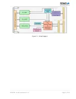
1 Product Description
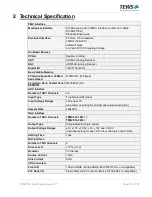
The TPMC533 is a standard single-wide PCI Mezzanine Card (PMC) compatible module providing 32
channels of simultaneous sampling true differential bipolar 16bit analog input, 16 or no channels of
simultaneous update single-ended unipolar/bipolar 16bit analog output and 8 channels of tri-state 5V-tolerant
TTL digital input/output. All signals are accessible through a HDRA100 type front I/O connector.
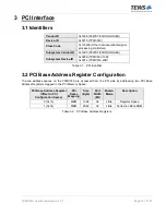
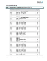
The PMC-Connectors P11 and P12 provide access to the control logic via a 32bit 33MHz PCI interface.
The ADCs offer true differential inputs with software selectable ±5V and ±10V bipolar input voltage ranges
(one common setting for all eight channels of each ADC). The maximum sample rate of the ADCs is
200kSPS and they offer an oversampling capability with digital filter.
The DACs offer software selectable 0-5V, 0-10V, 0-10.8V, ±5V, ±10V and ±10.8V output voltage ranges
(individual setting for each of the four channels of each D
AC). The settling time is typically 10μs and the DAC
channels are capable to drive a load of 2kΩ, with a capacitance up to 4000pF.
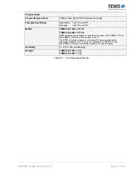
Each TPMC533 is factory calibrated. The correction data is stored in an on-board serial EEPROM unique to
each PMC module. These correction values can be used to perform a hardware correction of every analog-
to-digital and digital-to-analog conversion. Additionally, measurement data read out of a temperature sensor
on-board can be used to compensate temperature dependent errors.
The TPMC533 provides two Sequencers, one for AD Conversions and another one for DA Conversions. To
perform periodic simultaneous conversions the conversion rates are programmable and can be output to
other modules on PMC Back I/O Connector P14 or Front I/O Connector DIO pins for synchronization
purposes. The TPMC533 can also operate as a target which means that the conversion rates can be
sourced from P14 or Front I/O, created by another module.
A Frame Trigger signal, which can also either be generated by the TPMC533 and output on P14/Front I/O or
generated by other modules and input from P14/Front I/O, can be used to synchronize ADC frames and
DAC frames.
The signals on PMC Back I/O Connector P14 are ESD protected and driven or read by tri-state 5V-tolerant
TTL buffers.
To be able to collect ADC frames and to output DAC frames the TPMC533 provides input and output FIFOs.
Data transfer on the PCI bus is handled by TPMC533 initiated block transfer mode DMA cycles with
minimum host/CPU intervention.
The 8 Digital TTL tri-
state I/O lines with 4.7kΩ pull resistors are ESD protected. The voltage, the pull
resistors are connected to, is programmable by software and can be 3.3V, 5V, GND or floating level (one
common setting for all eight Digital I/Os). All 8 DIOs can be programmed whether to have their Digital I/O
transmitters enabled or disabled individually per I/O line. The Digital I/O receivers are always enabled, so
each DIO level can always be monitored and can generate an interrupt, triggered on rising edge, falling edge
or both. Additionally, a debounce filter can be configured to get rid of bounce on the Digital I/O lines.