


TPMC533 User Manual Issue 1.0.1
Page 88 of 107
Digital I/O and P14 Back I/O
4.3
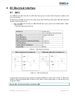
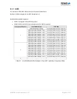
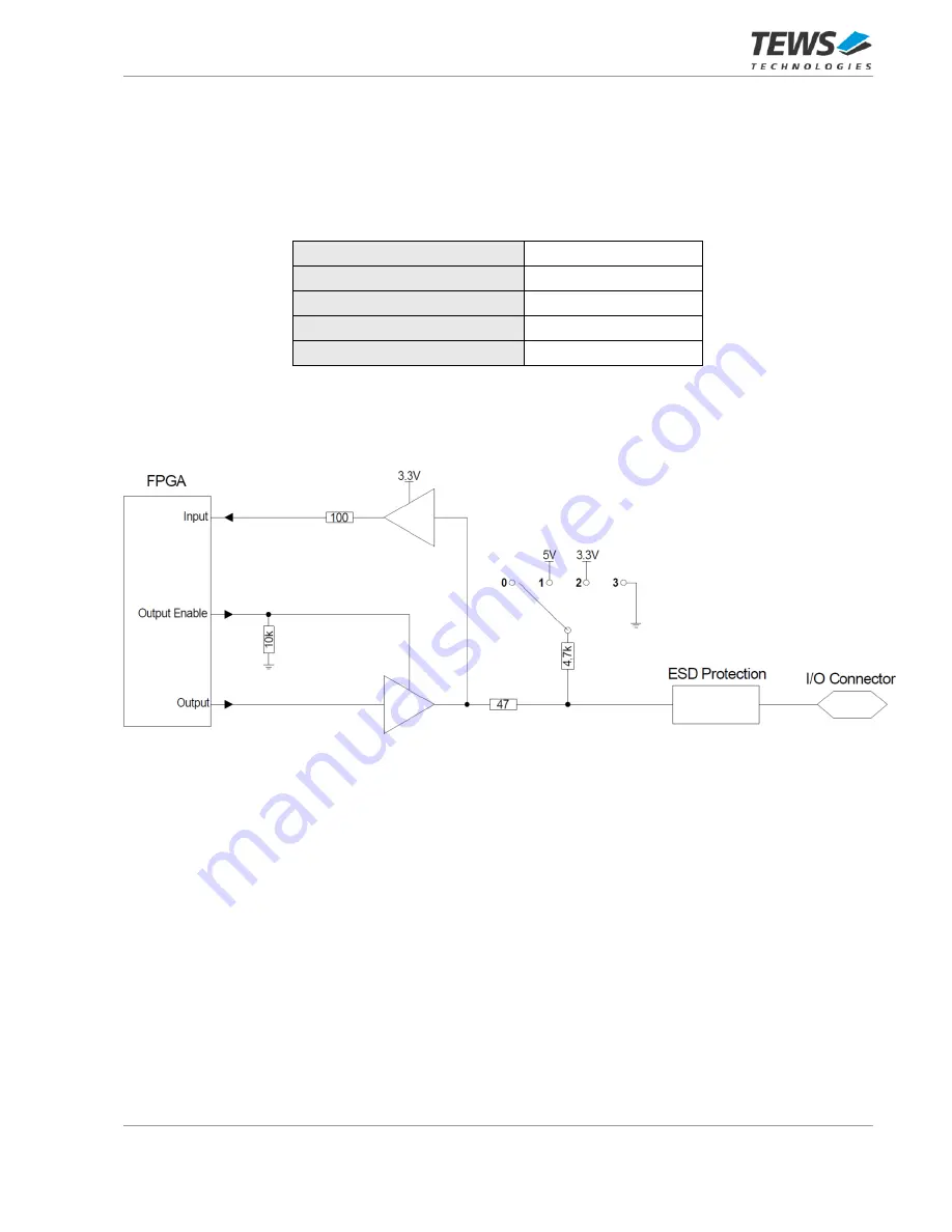
Each of the 8 Digital I/O lines on the Front I/O connector and each of the Global Conversion Signals on P14
Back I/O is realized by separated input and output buffers with a
4.7kΩ pull
resistor which can be used for tri-
state output functionality for example.
Additionally, each signal is equipped with an electronic protection array for ESD protection.
Protection
±15kV ESD protection
Driver Level
LVTTL (3.3V)
Receiver
5V tolerant
Source current per line
15mA
Sink current per line
6mA
Table 4-4 : Digital I/O and P14 Back I/O Electrical Interface
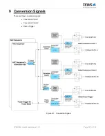
See the following figure for more information of the electrical circuitry.
Figure 4-1 : Digital I/O and P14 Back I/O Scheme
At power-up and after reset all Digital I/O and P14 Back I/O lines are configured as inputs. The pull resistors
are left floating (but they are still connected to each other) and have to be configured by software whether to
operate as pull-downs to GND or as pull-ups to +3.3V or +5V. This pull resistor setting can be configured
individually for DIO Front I/O and for P14 Back I/O.
The receiver function is always available and may be used to monitor the Digital I/O line level even when the
line is operating as an output.
To achieve a 5V CMOS high-level (V
OH
≥
3.5V), the external load must be high impedance and the pull
resistors must be configured to +5V pull-ups. The corresponding bit in the DIO Output Register must be set
to '0' while the DIO output level is controlled via the corresponding bit in the DIO Output Enable Register
('disabled' means logic high). To maintain a proper 5V CMOS high-level, the external load (leakage) current
should not exceed 250µA.
Each Digital I/O input is capable of generating an interrupt on either rising edge or falling edge and a
debounce filter can be configured to get rid of bounce on the Digital I/O Inputs.


