TPMC533 User Manual Issue 1.0.1
Page 99 of 107
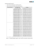
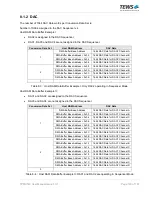
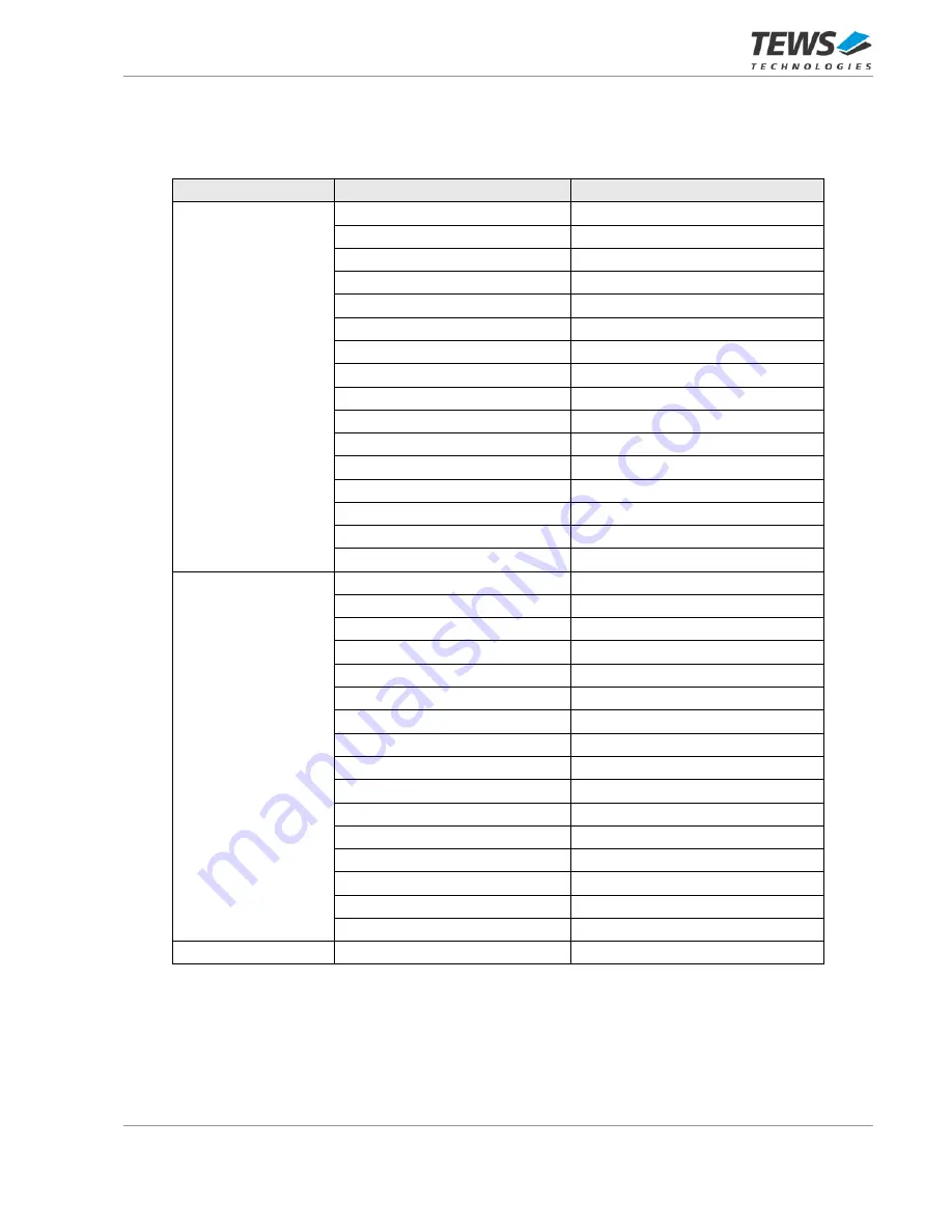
Host RAM Data Buffer Example II:
•
ADC1 and ADC2 are assigned to the ADC Sequencer.
•
ADC3 and ADC4 are not assigned to the ADC Sequencer.
Conversion Data Set
Host RAM Address
ADC Data
1
DMA Buffer Base Address
16bit ADC Data for ADC1 Channel A
DMA Buffer Base A 0x02
16bit ADC Data for ADC1 Channel B
DMA Buffer Base A 0x04
16bit ADC Data for ADC1 Channel C
DMA Buffer Base A 0x06
16bit ADC Data for ADC1 Channel D
DMA Buffer Base A 0x08
16bit ADC Data for ADC1 Channel E
DMA Buffer Base A 0x0A
16bit ADC Data for ADC1 Channel F
DMA Buffer Base A 0x0C
16bit ADC Data for ADC1 Channel G
DMA Buffer Base A 0x0E
16bit ADC Data for ADC1 Channel H
DMA Buffer Base A 0x10
16bit ADC Data for ADC2 Channel A
DMA Buffer Base A 0x12
16bit ADC Data for ADC2 Channel B
DMA Buffer Base A 0x14
16bit ADC Data for ADC2 Channel C
DMA Buffer Base A 0x16
16bit ADC Data for ADC2 Channel D
DMA Buffer Base A 0x18
16bit ADC Data for ADC2 Channel E
DMA Buffer Base A 0x1A
16bit ADC Data for ADC2 Channel F
DMA Buffer Base A 0x1C
16bit ADC Data for ADC2 Channel G
DMA Buffer Base A 0x1E
16bit ADC Data for ADC2 Channel H
2
DMA Buffer Base A 0x20
16bit ADC Data for ADC1 Channel A
DMA Buffer Base A 0x22
16bit ADC Data for ADC1 Channel B
DMA Buffer Base A 0x24
16bit ADC Data for ADC1 Channel C
DMA Buffer Base A 0x26
16bit ADC Data for ADC1 Channel D
DMA Buffer Base A 0x28
16bit ADC Data for ADC1 Channel E
DMA Buffer Base A 0x2A
16bit ADC Data for ADC1 Channel F
DMA Buffer Base A 0x2C
16bit ADC Data for ADC1 Channel G
DMA Buffer Base A 0x2E
16bit ADC Data for ADC1 Channel H
DMA Buffer Base A 0x30
16bit ADC Data for ADC2 Channel A
DMA Buffer Base A 0x32
16bit ADC Data for ADC2 Channel B
DMA Buffer Base A 0x34
16bit ADC Data for ADC2 Channel C
DMA Buffer Base A 0x36
16bit ADC Data for ADC2 Channel D
DMA Buffer Base A 0x38
16bit ADC Data for ADC2 Channel E
DMA Buffer Base A 0x3A
16bit ADC Data for ADC2 Channel F
DMA Buffer Base A 0x3C
16bit ADC Data for ADC2 Channel G
DMA Buffer Base A 0x3E
16bit ADC Data for ADC2 Channel H
3
…
…
Table 8-2 : Host RAM Data Buffer Example II: ADC1 and ADC2 are operating in Sequencer Mode