4
Parallel EVM Site
4.1
Parallel Analog I/O and Power Connections
4.2
Parallel Control Connector—J18
www.ti.com
Parallel EVM Site
The parallel interface consists of a 48-pin header (J17), which provides access to up to 24 parallel data
bits and a 20-pin parallel control header (J18). The parallel control header provides four multiplexed
address lines, configurable read and write strobes, configurable interrupts, and chip-select and clock
signals. Analog I/O and power is also provided.
The parallel site uses the same analog I/O and power connections described in the serial interface section
of this manual. Typically, a parallel-ADC EVM uses the analog interface connector located at J10 and the
power connector located at JP5. See
for pinout details. A parallel-DAC EVM typically uses the
analog interface connector J12, presenting the opportunity to stack certain EVMs.
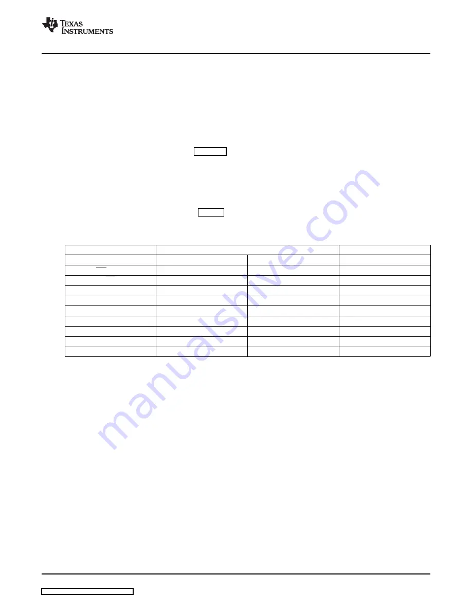
The parallel control connector feeds chip-select, read, write, and address lines to the parallel EVMs. The
address decoding for most parallel EVMs is done on the EVM card itself, allowing the possibility of
stacking several cards together. Table
shows the typical signals found on parallel interface EVMs,
designed to be used with the 5–6K Interface Board
Table 7. Parallel Control Connections
Signal
Pin Number
Signal
DC_CSx
1
2
DGND
WR (R/W)
3
4
DGND
RD
5
6
DGND
EVM_A0
7
8
DGND
EVM_A1
9
10
DGND
EVM_A2
11
12
DGND
EVM_A3
13
14
DGND
GPIO (SPARE–NC)
15
16
DGND
TOUTa
17
18
DGND
INT
19
20
DGND
DC_CSx is defined in the TMS320 Cross-Platform Daughtercard Specification. This signal is intended to
act as a chip-select to the EVM, not necessarily the actual data converter being evaluated. Carefully read
the documentation that came with your EVM for details on how this signal is used. Revision-B Interface
boards include jumper W16 which applies DC_CSa (default) or DC_CSb (shunt pins 2-3) to J18 pin 1.
The write and read strobes can be controlled through jumpers W4 and W5 on the Interface Card. With W4
and W5 in their default positions (shunt on pins 2-3), WR and RD are defined as in the TMS320
Cross-Platform Daughtercard Specification. With the shunts on W4 and W5 in positions 1-2, combination
logic located on the interface card can provide a simple strobing arrangement which may be useful with
the TMS320C5402 DSK.
The EVM address lines EVM_A0 through EVM_A3 are fed from a four-bit 2:1 bus switch, U1. Typically,
this provides access to DSP address lines A2..A5, or A14..A17. A shunt on W1 (default) applies the DSK
address lines A2..A4 to the parallel control connector; removing the shunt from W1 applies address lines
A14..A17. The actual address lines vary depending on the DSK used; see your DSK documentation for
the exact address locations.
SLAU104C – May 2004 – Revised March 2009
List of Tables
5


