Introduction
The on-board jumper options allow configuration of on-board power supplies and ADC options. Many of
the jumper selections that involve DC inputs or static control signals are by way of push-on square post
jumpers. The jumper options are listed in
indicates the default settings of the jumpers as
the EVM is normally shipped.
Table 4. ADC3xxxx EVM Jumper Options
Device
Jumper
Description
ADC32xx/ADC34xx
JP1
3 pin Jumper – 2-3 Default connection, 1-2 to enable PwDn function
JP2, J3, JP4,JP5
2 pin Jumper - SPI access points, if needed – default should be installed
ADC32J/34Jxx
JP1
3 pin Jumper – 2-3 Default connection, 1-2 to enable PwDn function
JP2, J3, JP4,JP5
2 pin Jumper - SPI access points, if needed – default should be installed
JP6
2 pin, default is connected for powering onboard VCXO
SJP1
3 pin, DNI, optional for VCXO that require enable on pin 2
JP11
2 pin, normally connected to enable current monitor for 1.8-V supply to ADC
JP8
3 pin, default 2-3 for USB SPI selection through CPLD, 1-2 used for FMC
connector based SPI port
There is a pushbutton on the ADC3xxxx EVM –
SW1
. Upon powering up, the ADC can either accept
hardware reset by pressing
SW1
or toggling the software reset switch on the ADC3xxxx EVM GUI. The
default reset configuration of the ADC is given in its respective data sheet.
LED D1 on the ADC32/34xxx is lit to show the presence of the 5-V supply voltage to the EVM. On the
ADC32J/34Jxx EVMs, LED D8 is used to show the presence of the 5-V supply voltage to the EVM.
lists the description of each LED indicator.
Table 5. ADC3xxxx EVM LED Indicators
Device
LED
Description
ADC32xx/ADC
D1
5-V power indicator
34xx
ADC32J/34Jxx
D1, D2
Status LED from CLKin SEL0/1 on LMK
D3, D4
Status LED used to indicate LMK Lock or PLL Lock
D5
Status LED for JESD SYNC
D6, D7
Spare LED indicators for FMC connector
D8
5-V power indicator
1.4
EVM ADC Input Circuit Configurations
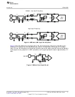
shows the ADC3xxxx ADC input circuit. The default setup has a dual 1:1 impedance ratio
transformer input circuit to achieve better phase and amplitude balance of the input signal than would
typically be produced by a single transformer input circuit.
The default input termination is 50
Ω
, which is formed by two 25-
Ω
resistors connected to the ADC VCM
node. By default the input circuit is set for operation within the 1st 2 Nyquist zones. For higher frequency
inputs use the high frequency input circuit as shown in
.
10
ADC3xxx, ADC3xJxx EVM User’s Guide
SLAU579A – June 2014 – Revised September 2014
Copyright © 2014, Texas Instruments Incorporated


