background image

www.ti.com

Basic Test Procedure

3.5

Test Set-up Connection (Onboard LMK04828 Clock)

1. Connect J17 connector of ADC32Jxx/ADC34Jxx EVM to J4 connector of TSW14J56 EVM revB

2. Connect 5V to the J11 supply input connector of the TSW14J56 and 5V to the J20 supply input

connector of the ADC32Jxx/34Jxx EVM

3. Connect a USB cable from the ADC32J/34Jxx EVM to the PC for SPI programming. The

ADC32J/34Jxx EVMs require some programming for the on board clock requirements of the
JESD204B interface.

4. Provide a sine wave for the analog input at J3 or J6 of ADC32Jxx EVM and J1, J3, J5, or J7 of the

ADC34Jxx EVM.

5. Connect USB cable from the TSW14J56 to the programming computer

6. Verify the following jumper connections on the ADC32J/34Jxx EVM

JP1 – 1,2 default condition PDN is low

JP2, JP3, JP4, JP5 – closed – default condition for SPI connection

JP6 – Closed – power for the onboard clock

JP8 – 2,3 – default condition to select USB port for SPI communication

JP9 – 1,2 – default condition select LDO power

JP10 – 1,2 – default condition select LDO power

JP12 – 1,2 – default condition select LDO power

JP13 – 1,2 – default condition select LDO power

25

SLAU579A – June 2014 – Revised September 2014

ADC3xxx, ADC3xJxx EVM User’s Guide

Submit Documentation Feedback

Copyright © 2014, Texas Instruments Incorporated

Summary of Contents for ADC3 J EVM Series

Page 1: ...oftware Control 12 2 1 Installation Instructions 12 2 2 Software Operation 12 3 Basic Test Procedure 21 3 1 Test Block Diagram with ADC32xx and ADC34xx 21 3 2 Test Set up Connection 22 3 3 ADC32 34xx and TSW1400 Setup Guide 22 3 4 Test Block Diagram with ADC32Jxx and ADC34Jxx 24 3 5 Test Set up Connection Onboard LMK04828 Clock 25 3 6 ADC32J 34Jxx and TSW14J56 Setup Guide 26 List of Figures 1 Simp...

Page 2: ...t Signal 27 List of Tables 1 ADC3xxx Family of Parts and EVMs 3 2 Power Supply Options 7 3 ADC3xxxx EVM Connectors 9 4 ADC3xxxx EVM Jumper Options 10 5 ADC3xxxx EVM LED Indicators 10 2 ADC3xxx ADC3xJxx EVM User s Guide SLAU579A June 2014 Revised September 2014 Submit Documentation Feedback Copyright 2014 Texas Instruments Incorporated ...

Page 3: ...VM 1 ADC34J44 14 125 ADC34J44EVM ADC34J45 14 160 ADC34J45EVM 1 EVM is scheduled for release at a later date There are 3 package sizes and pinouts for all of these parts The sLVDS dual devices use a 7 7 mm 48 pin QFN the sLVDS quad devices use an 8 8 mm 56 pin QFN and the dual and quad JESD204B device share the same package using a 7 7 mm 48 pin QFN The Dual ADCs comprise 2 buffered inputs 2 ADC co...

Page 4: ...supplied to the EVM through a single ended SMA connection then transformer coupled to turn the single ended signal into a balanced differential signal and then input to the ADC32xxx or ADC34xxx A dual transformer input circuit is used for better phase and amplitude balance of the input signal than would typically be produced by a single transformer input circuit Figure 1 Simplified ADC344x EVM Blo...

Page 5: ...nal to an SMA connector and transformer coupled to produce a differential clock signal for the ADC32 34xx EVM For the ADC32J 34Jxx EVM the clock input can be generated on board using the LMK04828 Power to the ADC3xxx EVM is typically supplied by a single 5 V connection by way of a 5 V power brick All necessary voltages for the ADC EVM are derived from the 5 V input connection 5 SLAU579A June 2014 ...

Page 6: ...4828 1 Low Noise LDO Introduction www ti com 1 2 EVM Power Supply Figure 3 illustrates the power supply options available on the ADC3xxx EVM Jumpers are used to choose the power supply options with the default jumper positions indicated by the darker portion of the jumper that represents the presence of the jumper Refer to Table 2 for jumper and feedback resistor configuration Figure 3 Simplified ...

Page 7: ...efault power path has an efficient dual output DC DC switching power supply to first step down the input supplies from 5 V to 4 V and 2 8 V for the subsequent low noise LDOs The 4 V is used by an LDO to derive 3 3 V for the LMK04828 clock circuits on the ADC3xJxx EVMs The 2 8 V is used by an LDO to derive a 1 8 V supply for the ADC and USB circuits The low noise LDOs can be bypassed to allow the D...

Page 8: ...ically the ADC inputs are transformer coupled to accept single ended connections The input circuit can be configured to connect to two SMA connectors for differential signaling if desired Table 3 lists the connector information for the ADC3xxxx 8 ADC3xxx ADC3xJxx EVM User s Guide SLAU579A June 2014 Revised September 2014 Submit Documentation Feedback Copyright 2014 Texas Instruments Incorporated ...

Page 9: ...C data connector to TSW1400 evaluation platform J14 Mini USB connector for SPI control J15 Power connector for 5 V adapter ADC32J 34Jxx J1 AIN_CH AP positive input for CHA single ended input DNI for ADC32Jxx J2 AIN_CH AM negative input DNI for ADC32Jxx J3 BIN_CH BP positive input for CHB CHA input for ADC32Jxx single ended input J4 BIN_CH BM negative input for CHB CHA input for ADC32Jxx J5 CIN_CH ...

Page 10: ...tware reset switch on the ADC3xxxx EVM GUI The default reset configuration of the ADC is given in its respective data sheet LED D1 on the ADC32 34xxx is lit to show the presence of the 5 V supply voltage to the EVM On the ADC32J 34Jxx EVMs LED D8 is used to show the presence of the 5 V supply voltage to the EVM Table 5 lists the description of each LED indicator Table 5 ADC3xxxx EVM LED Indicators...

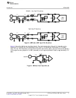
Page 11: ...circuit The clock signal will go through 1 4 impedance ratio transformer to increase the clock amplitude by two that is 1 4 impedance ratio equals to 1 2 voltage ratio The two 100 Ω resistors will impedance transform back to the primary side as 50 Ω load impedance for the signal source generator For ADC evaluation set the signal generator output to approximately 10 dBm Figure 7 DC34xx Clock Input ...

Page 12: ...op up screen opens select Continue Downloading b Follow the on screen instructions to install the USB drivers c If needed access the drivers directly in the install directory 2 2 Software Operation The software allows programming control of the ADC3xxxx device The front panel provides a tab for full programming of the register map of the ADC3xxxx and an advanced tab that allows for custom register...

Page 13: ...s to default configuration similar to pressing SW1 self clearing Global Power Down power down the entire chip default 0 ADC Standby All ADCs enter standby mode default 0 Configure PwDn pin function either global power down or ADC standby mode Data Format 0 2s Complement 1 Offset Binary default 0 Disable SYSREF BUF Disable SYSREF Buffer default 0 Clk Diver Internal clock divider to allow harmonic c...

Page 14: ...ign Test Data align all test data on the outputs Test Pattern CHA different available test patterns Test Pattern CHB different available test patterns Custom Pattern 14 bit custom bit pattern used when Custom Pattern is selected Disable Chopper CHA disable the chopper function which shifts 1 f nose to Fs 2 by default it is on Disable Chopper CHB disable the chopper function which shifts 1 f nose t...

Page 15: ... the use of test patterns instead of sample data Align Test Data align all test data on the outputs Test Pattern CHA different available test patterns Test Pattern CHB different available test patterns Test Pattern CHC different available test patterns Test Pattern CHD different available test patterns Custom Pattern 14 bit custom bit pattern used when Custom Pattern is selected Disable Chopper CH...

Page 16: ...oftware Control www ti com Figure 10 ADC34XX Tab 16 ADC3xxx ADC3xJxx EVM User s Guide SLAU579A June 2014 Revised September 2014 Submit Documentation Feedback Copyright 2014 Texas Instruments Incorporated ...

Page 17: ...ult Test Mode Enable option to enable long test pattern as per clause 5 1 6 3 Flip ADC Data normal operation is LSB first enable for MSB first Insert Lane Alignment Chars option to insert lane alignment chars as per clause 5 3 3 4 TX Link Config option to disable ILA when SYNC is de asserted Ctrl K default is 9 20x mode enable to use 0x31 for control Ctrl F default is 2 20x mode enable to use 0x30...

Page 18: ...ftware Control www ti com Figure 11 ADC32Jxx Tab 18 ADC3xxx ADC3xJxx EVM User s Guide SLAU579A June 2014 Revised September 2014 Submit Documentation Feedback Copyright 2014 Texas Instruments Incorporated ...

Page 19: ...ns Test Pattern CHD different available test patterns Custom Pattern 14 bit custom bit pattern to be used when Custom Pattern is selected SerDes Test Pattern available test patterns at the SerDes block Idle Sync Pattern pattern used for SYNC request K28 5 default Test Mode Enable option to enable long test pattern as per clause 5 1 6 3 Flip ADC Data normal operation is LSB first enable for MSB fir...

Page 20: ...s Sample configuration files for common frequency plans are located in the install directory Select the Load Regs button Double click on the data folder Double click on the desired register file Click on Send All to ensure all the values are loaded properly 2 2 3 Misc Settings Reconnect FTDI Toggle this button if the USB port is not responding This generates a new USB handle address NOTE Reset the...

Page 21: ... the evaluation setup involves a clock from a high quality signal generator and a sine wave for the analog input from a high quality signal generator High order narrow bandpass filters are usually required on clock and input frequencies to remove phase noise and harmonic content from the input sine waves If the two signal generators are not synchronized by an external reference signal to make the ...

Page 22: ...Data Converter Pro software version 2 6 or higher with TSW1400 hardware of Rev D or higher Single tone FFT test 1 Start the HSDC Pro GUI program When the program starts select the ADC tab and then select ADC324x_2W_14bit ini or ADC344x_2W_14bit ini device in the Select ADC drop down menu Figure 14 Select ADC32xx or 34xx in the HSDC Pro GUI Program 2 When prompted with Load ADC Firmware select YES ...

Page 23: ...Signal If the basic capture at this point is correct then the front panel options of the SPI GUI and the front panel options of the TSW1400 GUI may be varied as desired to test out different device options 23 SLAU579A June 2014 Revised September 2014 ADC3xxx ADC3xJxx EVM User s Guide Submit Documentation Feedback Copyright 2014 Texas Instruments Incorporated ...

Page 24: ... board clock chip LMK04828 and a sine wave for the analog input from a high quality signal generator High order narrow bandpass filters are usually required to remove phase noise and harmonic content from the input sine waves Since the on board clock and input sinewave are not coherent then the resulting FFT will need to have a windowing function such as Blackman Harris Hamming Hanning applied to ...

Page 25: ...t J3 or J6 of ADC32Jxx EVM and J1 J3 J5 or J7 of the ADC34Jxx EVM 5 Connect USB cable from the TSW14J56 to the programming computer 6 Verify the following jumper connections on the ADC32J 34Jxx EVM JP1 1 2 default condition PDN is low JP2 JP3 JP4 JP5 closed default condition for SPI connection JP6 Closed power for the onboard clock JP8 2 3 default condition to select USB port for SPI communication...

Page 26: ...g generated 2 Start the HSDC Pro GUI program When the program starts select the ADC tab and then select ADC32Jxx_LMF_222 or ADC34Jxx_LMF_442 device in the Select ADC drop down menu Figure 17 Select ADC32Jxx or 34Jxx in the HSDC Pro GUI Program 3 When prompted by Load ADC Firmware select YES 4 Select Single Tone FFT Test under Test Selection 5 Select the number of sample points and resulting number...

Page 27: ...4J25EVM and ADC34J44EVM in Table 1 3 Added ADC32J22EVM ADC32J42EVM ADC34J22EVM ADC34J42EVM to ADC3xxx Family of Parts and EVMs table 3 Deleted last sentence in paragraph following Power Supply Options table 7 Deleted last sentence in the first paragraph on the page 10 Deleted entire paragraph preceding ADC3xxxx EVM Jumper Options table 10 Deleted several rows from ADC3xxxx EVM Jumper Options table...

Page 28: ...ring the warranty period to the address designated by TI and that are determined by TI not to conform to such warranty If TI elects to repair or replace such EVM TI shall have a reasonable time to repair such EVM or provide replacements Repaired EVMs shall be warranted for the remainder of the original warranty period Replaced EVMs shall be warranted for a new full ninety 90 day warranty period 3 ...

Page 29: ...io transmitter has been approved by Industry Canada to operate with the antenna types listed in the user guide with the maximum permissible gain and required antenna impedance for each antenna type indicated Antenna types not included in this list having a gain greater than the maximum gain indicated for that type are strictly prohibited for use with this device Concernant les EVMs avec antennes d...

Page 30: ... any load to the EVM output If there is uncertainty as to the load specification please contact a TI field representative During normal operation even with the inputs and outputs kept within the specified allowable ranges some circuit components may have elevated case temperatures These components include but are not limited to linear regulators switching transistors pass transistors current sense...

Page 31: ...F REMOVAL OR REINSTALLATION ANCILLARY COSTS TO THE PROCUREMENT OF SUBSTITUTE GOODS OR SERVICES RETESTING OUTSIDE COMPUTER TIME LABOR COSTS LOSS OF GOODWILL LOSS OF PROFITS LOSS OF SAVINGS LOSS OF USE LOSS OF DATA OR BUSINESS INTERRUPTION NO CLAIM SUIT OR ACTION SHALL BE BROUGHT AGAINST TI MORE THAN ONE YEAR AFTER THE RELATED CAUSE OF ACTION HAS OCCURRED 8 2 Specific Limitations IN NO EVENT SHALL T...

Page 32: ...esponsible for compliance with all legal regulatory and safety related requirements concerning its products and any use of TI components in its applications notwithstanding any applications related information or support that may be provided by TI Buyer represents and agrees that it has all the necessary expertise to create and implement safeguards which anticipate dangerous consequences of failur...

Page 33: ...Information Texas Instruments ADC32J45EVM ADC3444EVM ADC34J25EVM ADC3224EVM ADC34J44EVM ADC3424EVM ADC34J43EVM ADC3223EVM ADC34J23EVM ADC3241EVM ADC3442EVM ADC3243EVM ADC34J24EVM ADC3242EVM ADC3222EVM ADC32J23EVM ADC32J25EVM ADC32J24EVM ADC32J42EVM ADC32J43EVM ADC32J44EVM ADC3421EVM ADC3423EVM ...

Reviews: