Introduction
Table 2. Power Supply Options
Device
Description
ADC32xx
Default connection for LDO 1.8-V supply, switch both to 2-3 to use the switcher U4, install R79 for 1.8-V
JP6: 1-2, JP7: 1-2
switcher output
ADC34xx
Default connection for LDO 1.8-V supply, switch both to 2-3 to use the switcher U4, install R79 for 1.8-V
JP6: 1-2, JP7: 1-2
switcher output
ADC342J/34Jxx
spacer
JP9: 1-2, JP10: 1-2
Default connection for LDO 1.8-V supply, switch both to 2-3 to use the switcher U8, install R152 for 1.8-V
spacer
switcher output
spacer
spacer
JP12: 1-2, JP13: 1-2
Default Connection for LDO 3.3 V for LMK04828 power and onboard SPI/CPLD, switch both to 2-3 to use
U11 switcher output, install R163 for 3.3-V switcher output
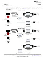
The default power path has an efficient dual output DC-DC switching power supply to first step down the
input supplies from 5 V to 4 V and 2.8 V for the subsequent low noise LDOs. The 4 V is used by an LDO
to derive 3.3 V for the LMK04828 clock circuits on the ADC3xJxx EVMs. The 2.8 V is used by an LDO to
derive a 1.8-V supply for the ADC and USB circuits.
The low noise LDOs can be bypassed to allow the DC/DC power supply to directly provide the ADC
power. Please note that the feedback resistors of the DC/DC converter need to be adjusted accordingly.
Refer to the ADC EVM schematic for details.
1.3
EVM Connectors and Jumpers
and
show the locations of the connectors, jumpers, pushbutton switches, and LED.
Figure 4. ADC34Jxx EVM Connector and Jumper Locations
7
SLAU579A – June 2014 – Revised September 2014
ADC3xxx, ADC3xJxx EVM User’s Guide
Copyright © 2014, Texas Instruments Incorporated


