


GND
TLV320ADC5140DC087A
GND
AVDD
IOVDD
GND
J5
ADD0/SCLK
GND
GND
ADD1/MISO
GND
16V
0.1uF
C1
16V
0.1uF
C3
SHDNz
DOUT
BCLK
FSYNC
GPIO1
MICBIAS
GND
GND
GND
J6
J8
J9
J10
J11
J12
J7
IN1P
IN1M
IN2P
IN2M
IN3P
IN3M
IN4P
IN4M
16V
0.1uF
C7
16V
0.1uF
C9
GND
GND
GND
GND
16V
1uF
C5
GND
GND
ADD0/SCLK
ADD1/MISO
IOVDD-MB
IOVDD-MB
GND
GND
R12
R10
2.2k
R13
2.2k
R11
Control Interface Selection
GPIO1
GND
MCLK
INTz
R3
GPIO1 Selection
J13
GPIO1
VREF
AREG
DREG
TP1
IN1P
TP2
IN1M
TP3
IN2P
TP4
IN2M
TP5
IN3P
TP6
IN3M
TP7
IN4P
TP8
IN4M
GND
0
R1
GPIO1 is optional for MCLK or INTz
TLV320AICx140 CIRCUIT
TLV320A DC5140IRTWR
10
IN3P_GPI3
9
1
IN2M_GPO2
AVDD
20
GPIO1
19
IOVDD
3
VREF
BCLK
22
23
FSYNC
15
ADDR1_MISO
16
ADDR0_SCLK
8
IN2P_GPI2
11
IN3M_GPO3
7
IN1M_GPO1
12
IN4P_GPI4
6
IN1P_GPI1
13
IN4M_GPO4
21
SDOUT
24
DREG
5
MICBIAS
14
SHDNZ
4
AVSS
17
SCL_MOSI
18
SDA_SSZ
2
AREG
VSS
25
U1
IN1P_GPI1
IN2P_GPI2
IN3P_GPI3
IN4P_GPI4
IN1M_GPO1
IN2M_GPO2
IN3M_GPO3
IN4M_GPO4
MICBIAS
IOVDD-MB
IOVDD
GND
TP9
GND
TP10
GND
AVDD
GND
+3.3V
TP16
MICBIAS
MICBIAS
TP11
AVDD
AVDD
TP12
IOVDD
IOVDD
JMP1
JMP2
Power Test Points
VREF
AREG
DREG
TP13
AREG
TP14
DREG
TP15
VREF
SCL/MOSI
SDA/SSZ
SCL/MOSI
SDA/SSZ
R6
0
R8
R5
R4
SCL
SDA
MISO
MOSI
SCLK
SS0
R7
0
R9
From DUT
SPI
I²C
R2
MICBIAS
J15
J16
IN1P
IN1M
GND
1
VDD
3
OUT+
4
GND
2
OUT-
MK1
AMIC1P
AMIC1M
J14
GND
16V
0.1uF
C11
On-Board Microphone
SCL
SDA
SS0
SCLK
MISO
MOSI
1
2
3
4
5
6
7
8
9
10
11
12
13
14
15
16
17
18
19
20
21
22
23
24
25
26
27
28
29
30
31
32
33
34
35
36
37
38
39
40
4
1
4
2
4
3
4
4
J17
GND
+5V
IOVDD-MB
DIN1
DOUT
MCLK
BCLK
FSYNC
DIN2
DOUT2
GPO2
GPI2
GND
GND
GPO1
DIN3
DIN4
DOUT3
DOUT4
SS1
Connector to A C-MB
INTz
TP17
IOVDD-MB
TP18
+5V
+5V
IOVDD-MB
RSTz
SHDNz
RSTz
GND
GND
+5V
GND
GND
+3.3V
GND
1
OUT
NC
2
3
NR
4
GND
5
EN
6
NC
7
NC
IN
8
9
PAD
U2
TPS735xxDRB-Q1
GND
GND
16V
0.1uF
C13
16V
10uF
C12
16V
0.1uF
C23
16V
10uF
C24
16V
C22
0.01uF
On-Board +3.3V Power Supply
1
Green
2
D1
442
R15
+3.3V
Power
Power LED
GND
A0
1
2
A1
3
A2
4
VSS
5
SDA
6
SCL
WP
7
8
VCC
U3
24LC512-I/ST
IOVDD-MB
IOVDD-MB
SCL
SDA
2.2k
R16
16V
0.1uF
C25
GND
GND
GND
EEPROM for Firmw are ID
2.2k
R17
IOVDD-MB
2.2k
R18
External RST Option
From Motherboard
To DUT
0
R14
Main
Digital Signal Test Points
SHDNz
DOUT
MCLK
BCLK
FSYNC
SCL
SDA
TP25
SHDNz
TP21
DOUT
TP19
FSYNC
TP20
BCLK
TP22
MCLK
TP23
SCL
TP24
SDA
INTz
TP26
INTz
MISO
MOSI
TP27
MISO
TP28
MOSI
SCLK
TP29
SCLK
SS0
TP30
SS0
From DUT
From Motherboard
To DUT
Jumper Description
J14
Designator
I²C Address
J15
J16
J5-J12
Function
MICBIAS Connection to On-Board Mic
IN1P Connection to On-Board Mic
IN1M Connection to On-Board Mic
Designator
Function
J13
Capacitor Bypass for direct connection from
DUT input pins to input terminals
Connection to DUT GPO
1
2
3
J1
1
2
3
J2
Populate resistors according to
the desired control interface
1
2
3
J3
1
2
3
J4
16V
4.7uF
C14
16V
4.7uF
C15
16V
4.7uF
C16
16V
4.7uF
C17
16V
4.7uF
C18
16V
4.7uF
C19
16V
4.7uF
C20
16V
4.7uF
C21
16V
1uF
C2
10V
10uF
C8
10V
10uF
C10
10V
10uF
C4
16V
1uF
C6
Schematic and Bill of Materials
21
SBAU335 – May 2019
Copyright © 2019, Texas Instruments Incorporated
ADCx140EVM-PDK
6
Schematic and Bill of Materials
6.1
ADCx140EVM-PDK Schematic and Bill of Materials
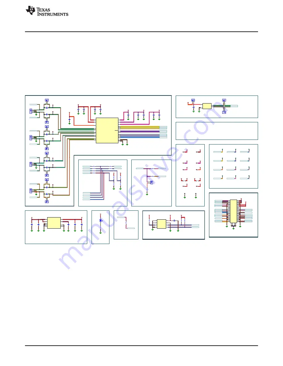
This section provides the schematics and bill of materials (BOM) for the ADCx140EVM-PDK.
6.1.1
ADCx140EVM-PDK Schematic
shows the schematics for the ADCx140EVM-PDK.
Figure 25. ADCx140EVM-PDK Schematics


