background image

X-SCL

X-SDA

X-SDA

X-SCL

S/PDIF-OUT

9211-BCLK

9211-FSYNC

9211-DOUT

1

ERROR/INT0

2

NPCM/INT1

3

MPIO_A0

4

MPIO_A1

5

MPIO_A2

6

MPIO_A3

7

MPIO_C0

8

MPIO_C1

9

MPIO_C2

10

MPIO_C3

11

MPIO_B0

12

MPIO_B1

13

MPIO_B2

14

MPIO_B3

MPO0

15

MPO1

16

DOUT

17

18

FSYNC

BCK

19

20

SCKO

21

DGND

22

DVDD

23

MDO/ADR0

24

MDI/SDA

25

MC/SCL

26

MS/ADR1

27

MODE

28

RXIN7/ADIN0

29

RXIN6/AFSYNCI0

30

RXIN5/ABCKI0

31

RXIN4/ASCKI0

32

RXIN3

33

RXIN2

RST

34

35

RXIN1

36

VDDRX

37

RXIN0

38

GNDRX

XTI

39

XTO

40

41

AGND

VCC

42

FILT

43

44

VCOM

45

AGNDAD

46

VCCAD

VINL

47

VINR

48

U11

PCM9211PT

1

VIN

2

V

C

C

3

G

N

D

N

C

4

5

N

C

U9

1

PLT133/T10W

V

C

C

2

G

N

D

3

VOUT

4

N

C

N

C

5

U13

PLR135/T10

GND

GND

16V

0.1uF

C56

+3.3V

GND

16V

0.1uF

C57

+3.3V

GND

GND

GND

1
3

4

2

G
G

Y2

24.576MHz

GND

50V

27pF

C49

GND

GND

50V

27pF

C48

16V

0.1uF

C53

16V

10uF

C52

25V

C54

4700pF

50V
0.068uF

C55

680

R44

EVM-RSTz

9211-MCLK
9211-BCLK

9211-FSYNC

9211-DOUT

9211-DIN

S/PDIF-IN

9211-MCLK

5
3

2

1

4

J6

GND

200k

R42

200k

R43

+3.3V

GND

GND

9211-LOCK

GND

PCM9211 Circuit

2

Blue

1

D5

16V

0.1uF

C64

GND

+3.3V

IOVDD

I2S-SEL-S0

+3.3V

AC-MB-MCLK

AC-MB-BCLK

AC-MB-FSYNC

AC-MB-DOUT1

AC-MB-DIN1

I2S-SEL-S0
I2S-SEL-S1

+3.3V

IOVDD

X-DIN1

X-DOUT1

X-MCLK
X-BCLK

X-FSYNC

9211-MCLK
9211-BCLK

9211-FSYNC

9211-DOUT

S

9211-DIN1

1

2

1B1

3

1B2

4

1A

5

2B1

6

2B2

8

GND

9

3A

3B2

10

3B1

11

4A

12

4B2

13

4B1

14

7

2A

OE

15

VCC

16

U10

SN74CB3Q3257DGVR

I2S-SEL-S1

+3.3V

GND

9211-BCLK

9211-FSYNC

9211-DOUT

9211-DIN1

9211-MCLK

X-MCLK

X-BCLK

X-FSYNC

X-DOUT1

X-DIN1

+3.3V

IOVDD

GND

EVM-MCLK

EVM-BCLK

EVM-FSYNC

EVM-DOUT1

EVM-DIN1

EVM-DIN1

EVM-DOUT1

EVM-MCLK

EVM-BCLK

EVM-FSYNC

EVM-SCL

EVM-SDA

10.0k

R45

+3.3V

X-SPI-SS0

X-SPI-CLK

X-SPI-MISO

X-SPI-MOSI

+3.3V

IOVDD

EVM-SPI-SS0

EVM-SPI-CLK

EVM-SPI-MISO

EVM-SPI-MOSI

GND

GND

Digital Audio Mux/Translation

+3.3V

16V

0.1uF

C62

16V

10uF

C63

GND

GND

16V

0.1uF

C59

16V

10uF

C58

GND

GND

GND

GND

+5V

+3.3V

16V

0.1uF

C60

16V

10uF

C61

L4

100 ohm

+5V-PCM

+5V-PCM

+3.3V

+3.3V

+5V-PCM

+3.3V

+5V-PCM

+3.3V

+3.3V

+3.3V

+3.3V

GND

16V

0.1uF

C74

+3.3V

GND

16V

0.1uF

C78

+3.3V

GND

16V

0.1uF

C75

GND

16V

0.1uF

C79

IOVDD

IOVDD

GND

16V

0.1uF

C66

+3.3V

GND

16V

0.1uF

C69

+3.3V

GND

16V

0.1uF

C67

GND

16V

0.1uF

C70

IOVDD

IOVDD

GND

16V

0.1uF

C65

+3.3V

GND

16V

0.1uF

C68

+3.3V

10.0k

R46

10.0k

R47

GND

+3.3V

+3.3V

Control Interface Translation

Analog

Optical

Input

Optical

Input

Output

I²C Translator

SPI Translator

Digital Aud io Mux

S/PDIF Lock

Digital Aud io Translator / Buffer

VINR

Aud io Conver ters Motherboard DC058 Rev A

PCM9211, Aud io Interface and Test Po ints

VINL

GND

GND

GND

GND

GND

GND

X-P0

X-P1

RSTz

S1

ON

ON

X

OFF

USB

S0

OPTICAL/ANALOG

AUDIO

EXTERNAL ASI

+3.3V

IOVDD

GND

EVM-RSTz

GND

GND

16V

0.1uF

C76

+3.3V

GND

16V

0.1uF

C77

IOVDD

SPI /  RST Translator

EVM-DIN2

EVM-DOUT2

S

1

2

1B1

3

1B2

4

1A

5

2B1

6

2B2

8

GND

3A

9

3B2

10

3B1

11

4A

12

4B2

13

4B1

14

7

2A

OE

15

VCC

16

U15

SN74CB3Q3257DGVR

I2S-SEL-S0

GND

GND

I2S-SEL-S1

GND

X-DIN2

9211-DOUT

9211-DIN2

9211-DIN2

R40

DNP

0

R39

9211-DIN1

2
1

9211-DIN2

3
4

SW2

A6SN-2104

X-SPI-SS1

EVM-SPI-SS1

EVM-GPO2

EVM-GPI2

EVM-GPO1

EVM-GPI1

X-P2

X-P3

+3.3V

IOVDD

GND

GND

GPIO Translator

EVM-DIN3

EVM-DOUT3

EVM-DIN4

EVM-DOUT4

EVM-DOUT2

EVM-DOUT4

EVM-DOUT3

EVM-DIN2

EVM-DIN3

EVM-DIN4

GND

X-DIN2
X-DIN3
X-DIN4

X-DOUT2
X-DOUT3
X-DOUT4

AC-MB-DOUT2

AC-MB-DIN2

AC-MB-DOUT3

AC-MB-DOUT4

AC-MB-DIN3

AC-MB-DIN4

TP15
+1V

DNP

+5V

TP1

+5V

DNP

+1.0V

+3.3V

+1.8V

TP14

TP2

+3.3V

DNP

+1.8V

DNP

GND

GND

GND

GND

GND

EVM-DIN1

EVM-DOUT1

EVM-MCLK
EVM-BCLK

EVM-FSYNC

EVM-SCL
EVM-SDA

EVM-SPI-SS0

EVM-SPI-CLK

EVM-SPI-MISO

EVM Connector

EVM-SPI-MOSI

Test Points

I²C

SPI

TP4
SCLK

DNP

TP6
MISO

DNP

TP11
MOSI

DNP

TP12
SS0

DNP

TP3
SCL

DNP

TP5
SDA

DNP

EVM-SPI-SS1

TP13
SS1

DNP

1

2

3

4

5

6

7

8

9

10

11

12

13

14

15

17

19

21

16

18

20

22

J7

EVM-DIN2
EVM-DIN3
EVM-DIN4

EVM-DOUT2
EVM-DOUT3
EVM-DOUT4

1

2

Extern al Aud io

3

4

5

6

7

8

9

10

11

12

13

14

15

16

17

18

19

20

21

22

23

24

25

26

27

28

29

30

31

32

33

34

35

36

37

38

39

40

4

1

4

2

4

3

4

4

J8

GND

+5V

IOVDD

EVM-DIN1

EVM-DOUT1

EVM-MCLK

EVM-BCLK

EVM-FSYNC

EVM-DIN2

EVM-DOUT2

EVM-GPO2

EVM-RSTz

EVM-GPI2

EVM-SPI-SS0

EVM-SPI-CLK

EVM-SPI-MISO
EVM-SPI-MOSI

EVM-SCL
EVM-SDA

GND

GND

EVM-SPI-SS1

EVM-GPO1

EVM-GPI1

EVM-DIN3
EVM-DIN4

EVM-DOUT3
EVM-DOUT4

X-DOUT3

X-DOUT4

X-DIN3

PSIA Connector

X-DIN4

GND

16V

0.1uF

C80

+3.3V

GND

16V

0.1uF

C81

IOVDD

Power

Audio Serial Interface Selection

SW2 Position

+3.3V

+3.3V

IOVDD

S

1

2

1B1

3

1B2

1A

4

5

2B1

6

2B2

8

GND

9

3A

3B2

10

3B1

11

4A

12

4B2

13

4B1

14

2A

7

OE

15

VCC

16

U17

SN74CB3Q3257DGVR

I2S-SEL-S0

GND

GND

I2S-SEL-S1

GND

16V

0.1uF

C72

+3.3V

GND

16V

0.1uF

C73

IOVDD

GND

16V

0.1uF

C71

+3.3V

GND

GND

GND

From XMOS

X-DOUT2

From PCM9211

16V

10uF

C50

16V

10uF

C51

O

ON

N

O

OF

FF

F

I2S-SEL-S0

I2S-SEL-S1

1

VCCA

2

SCLA

3

SDAA

4

GND

5

EN

6

SDAB

7

SCLB

8

VCCB

U20

TCA9802DGKR

TP7

GND

TP8

GND

TP9

GND

TP10

GND

1.5k

R41

2

4

U14A

5

VCC

SN74LVC1G14DCKR

3

GND

NC

1

U14B

DIR1

15

SN74AVC4T774RSVR

16

DIR2

1

A1

2

A2

3

A3

A4

4

5

DIR3

6

DIR4

OE

7

8

GND

9

B4

B3

10

B2

11

B1

12

VCCB

13

14

VCCA

U12

DIR1

15

SN74AVC4T774RSVR

DIR2

16

A1

1

2

A2

A3

3

4

A4

5

DIR3

6

DIR4

OE

7

8

GND

9

B4

B3

10

B2

11

B1

12

VCCB

13

14

VCCA

U16

DIR1

15

SN74AVC4T774RSVR

16

DIR2

1

A1

A2

2

A3

3

4

A4

5

DIR3

6

DIR4

OE

7

8

GND

B4

9

B3

10

B2

11

B1

12

VCCB

13

VCCA

14

U18

15

DIR1

SN74AVC4T774RSVR

16

DIR2

A1

1

A2

2

A3

3

4

A4

5

DIR3

6

DIR4

OE

7

8

GND

B4

9

B3

10

B2

11

B1

12

VCCB

13

14

VCCA

U19

15

DIR1

SN74AVC4T774RSVR

DIR2

16

A1

1

2

A2

3

A3

4

A4

5

DIR3

6

DIR4

OE

7

8

GND

B4

9

B3

10

B2

11

B1

12

13

VCCB

14

VCCA

U21

15

DIR1

SN74AVC4T774RSVR

16

DIR2

A1

1

A2

2

A3

3

A4

4

5

DIR3

6

DIR4

7

OE

8

GND

9

B4

B3

10

B2

11

B1

12

VCCB

13

VCCA

14

U22

Schematic and Bill of Materials

www.ti.com

24

SBAU335 – May 2019

Submit Documentation Feedback

Copyright © 2019, Texas Instruments Incorporated

ADCx140EVM-PDK

6.2

AC-MB Schematic and Bill of Materials

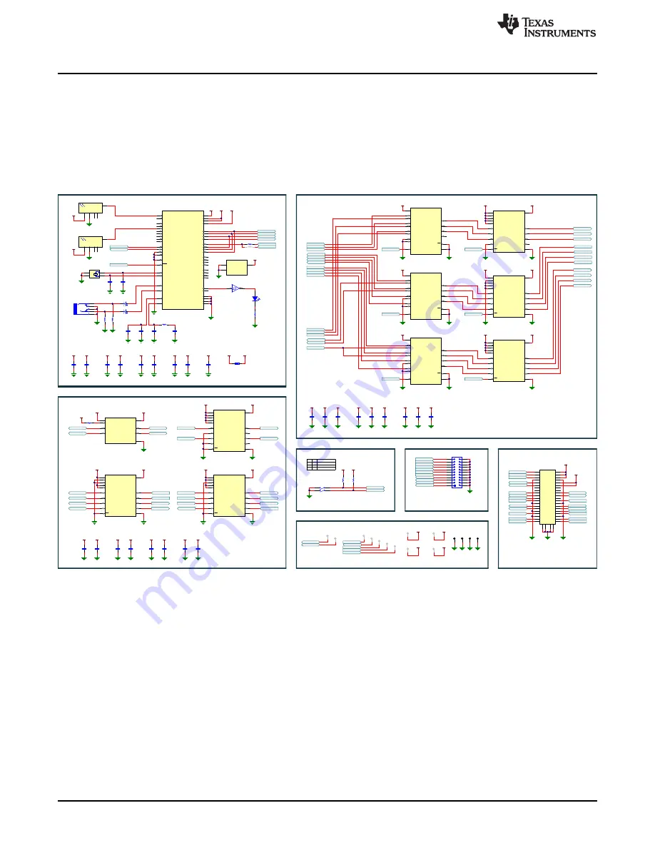
This section provides the schematics and BOM for the AC-MB.

6.2.1

AC-MB Schematic

Figure 26

shows the schematics for the ADCx140EVM-PDK.

Figure 26. AC-MB Schematics

Summary of Contents for ADC3140EVM-PDK

Page 1: ...nstructions a quick start guide jumper and connector descriptions software description schematics and printed circuit board PCB layout that demonstrate TI s recommended practices for these devices Contents 1 Introduction 3 2 Hardware Overview 3 2 1 AC MB Settings 3 2 2 ADCx140EVM PDK Hardware Settings 9 3 Software Overview 12 3 1 PurePath Console 3 Installation 12 3 2 ADCx140EVM GUI Installation 1...

Page 2: ... for Line Input Application 10 9 TLV320ADCx140EVB Connection for the Onboard Microphone Test 11 10 PurePath Console 3 Installation 12 11 PurePath Console 3 App Center 13 12 Initial GUI Configuration 13 13 Audio Config Tab 14 14 Hardware Connect 14 15 Audio Configuration 15 16 MIC Bias Configuration 15 17 Standby to Active Mode 15 18 Disabled Controls in Active Mode 16 19 Audio Serial Bus Tab 17 20...

Page 3: ...herboard is used to provide power control and digital audio signals to the evaluation module The daughterboard contains the TLV320ADCx140 device and its input connections A detailed functional overview of the TLV320ADCx140EVB system is described in Section 5 2 1 AC MB Settings 2 1 1 Audio Serial Interface Settings The AC MB provides the digital audio digital signals to the evaluation module from t...

Page 4: ...ing rate and format are determined by the USB audio class driver on the operating system The default settings for the USB audio interface are 32 bit frame size 48 kHz sampling rate BCLK and FSYNC ratio is 256 and the format is time division multiplexing TDM The AC MB is detected by the OS as an audio device with the name TI USB Audio UAC2 0 Figure 2 shows the AC MB audio setting for the USB mode o...

Page 5: ... Setting The optical output of the AC MB streams the data captured on the EVM with the format determined by the input source used When there is an optical input connected the LOCK LED must be ON and the PCM9211 streams the audio serial interface clocks with the format determined by the optical input frame The digital data from the optical input is streamed to the evaluation module If the optical i...

Page 6: ...e provided through connector J7 from an external source This architecture allows the use of an external system to communicate with the evaluation board such as a different host processor or test equipment for instance Audio Precision PSIA The clocks generated from the USB interface and PCM9211 are isolated with this setting Figure 4 shows the AC MB audio setting for the external mode of operation ...

Page 7: ...SBAU335 May 2019 Submit Documentation Feedback Copyright 2019 Texas Instruments Incorporated ADCx140EVM PDK Figure 5 shows how to connect the external audio interface with the bottom row for the signal and the top row for ground Figure 5 AC MB Connection with External Audio Serial Interface ...

Page 8: ...upply VBUS by shorting header J5 USB POWER Additionally the AC MB can be powered from an external power supply connected to terminal J4 EXTERNAL POWER Header J5 must be open for external supply operation The IOVDD voltage for the digital signals that is provided to the evaluation module is generated on the motherboard from the main power supply USB or external The voltage levels available are 1 8 ...

Page 9: ... configuration options and offers extensive flexibility to allow the user to evaluate the device across multiple operation modes The different operation modes are highlighted in this section The INxP and INxM pins of the TLV320ADCx140 can optionally connect to an onboard microphone for quick evaluation and can be optionally configured to bypass the input decoupling capacitors for evaluating the fu...

Page 10: ...or the line input configuration shown in Figure 8 the TLV320ADCx140 captures the audio signal provided through terminals J2 IN1 J3 IN2 J4 IN3 and J5 IN4 The input accepted in this mode is a differential 2 VRMS full scale audio signal If a single ended source is used the 1 VRMS signal is supported Figure 8 TLV320ADCx140EVB Connection for Line Input Application ...

Page 11: ...ut configuration shown in Figure 9 the TLV320ADCx140 records the audio captured from the microphones located on the bottom edge of the board MICBIAS is used to power the onboard microphone so header J14 must be shorted There must not be any connections to J1 during onboard microphone use to preserve the performance of the microphone Figure 9 TLV320ADCx140EVB Connection for the Onboard Microphone T...

Page 12: ... and debug process associated with the development of audio products 3 1 PurePath Console 3 Installation The ADCx140EVM PDK GUI is an application that installs into the PPC3 framework PPC3 must be installed prior to downloading the ADCX140EVM PDK GUI To download the PPC3 visit www ti com tool PUREPATHCONSOLE and request access If the PPC3 is already installed proceed to Section 3 2 Figure 10 shows...

Page 13: ...pen the PPC3 application in the directory chosen for the GUI installation in Section 3 1 Figure 11 shows the resulting app center window Click on the TLV320ADCx140 app tile Figure 11 PurePath Console 3 App Center The TLV320ADCx140 GUI is designed to work with up to four devices at any time As shown in Figure 12 choose the 1 device radial button and click New Figure 12 Initial GUI Configuration ...

Page 14: ...Before changing any parameters check the lower left corner of the PPC3 window as shown in Figure 14 to verify that the EVM is connected If no EVM is detected the text will read ADCx140 offline If the EVM is detected a Connect button appears Clicking this button connects the hardware Figure 14 Hardware Connect When the hardware is connected the Connect button changes to read Disconnect and the devi...

Page 15: ...udio configuration tab as shown in Figure 15 select a word length of 16 bits and enable the ASI output channel 1 Figure 15 Audio Configuration As shown in Figure 16 select AVDD for the MIC bias voltage and power up the MIC bias Figure 16 MIC Bias Configuration The default state for the TLV320ADCx140 is standby mode and with the exception of the channel digital volume all device configurations must...

Page 16: ...K When active mode is enabled any controls not configurable in active mode are grayed out These controls can be changed again when the device is brought out of active mode Figure 18 shows which controls are disabled Figure 18 Disabled Controls in Active Mode Audio can now be captured on your PC using the audio program of your choice ...

Page 17: ...s The default format is TDM however the GUI can be used to change the data format to I2 S This section describes how to configure the TLV320ADCx140EVM for a 2 channel I2 S output to a USB audio at 16 bits and 48 kHz Configure the AC MB for USB audio as described in Section 4 As shown in Figure 19 select the audio serial bus tab Figure 19 Audio Serial Bus Tab In the ASI format configuration pane sh...

Page 18: ...bus tab by clicking the Read button as shown in Figure 21 in the clock monitor pane Figure 21 Clock Monitor Pane The default slot assignment for channel 1 is left slot 0 and the default slot assignment for channel 2 is left slot 1 As shown in Figure 22 change the channel 2 slot assignment to right slot 0 The diagram at the top of the window updates to display the data format and slots selected Fig...

Page 19: ...uration To save a configuration as shown in Figure 23 click the upper left corner of the PPC3 window and select Save The configuration is saved as a ppc3 file To load a saved configuration click the upper left corner of the PPC3 window and select Open Navigate to the location of the saved ppc3 file and click Open Figure 23 Saving a Configuration in PPC3 ...

Page 20: ... S PDIF Output Stereo Analog Input PCM9211 Digital Interface Test Points ASI Selector External Power Terminal EVM Power Indicator DUT Circuit On Board Microphone Connection Headers Main System Reset Optical S PDIF Input EVM Power Indicator System Overview www ti com 20 SBAU335 May 2019 Submit Documentation Feedback Copyright 2019 Texas Instruments Incorporated ADCx140EVM PDK 5 System Overview Figu...

Page 21: ...S1 Connector to A C MB INTz TP17 IOVDD MB TP18 5V 5V IOVDD MB RSTz SHDNz RSTz GND GND 5V GND GND 3 3V GND 1 OUT NC 2 3 NR 4 GND 5 EN 6 NC 7 NC IN 8 9 PAD U2 TPS735xxDRB Q1 GND GND 16V 0 1uF C13 16V 10uF C12 16V 0 1uF C23 16V 10uF C24 16V C22 0 01uF On Board 3 3V Power Supply 1 Green 2 D1 442 R15 3 3V Power Power LED GND A0 1 2 A1 3 A2 4 VSS 5 SDA 6 SCL WP 7 8 VCC U3 24LC512 I ST IOVDD MB IOVDD MB ...

Page 22: ... OSTVN03A150 On Shore Technology J5 J6 J7 J8 J9 J10 J11 J12 J13 J14 J15 J16 12 Header 100mil 2x1 Gold 2x1 Header TSW 102 07 G S Samtec J17 1 Connector Header High Speed 20 pairs SMT QTE 020 01 X D A QTE 020 01 L D A Samtec JMP1 JMP2 2 Jumper Wire 100mil spacing Wire Jumper 923345 01 C 3M LBL1 1 Thermal Transfer Printable Labels 0 650 W x 0 200 H PCB Label 0 650 x 0 200 inch THT 14 423 10 Brady MK1...

Page 23: ... Bill of Materials continued Designator Qty Valu e Description Package Reference Part Number Manufacturer TP1 TP2 TP3 TP4 TP5 TP6 TP7 TP8 TP11 TP12 TP13 TP14 TP15 TP16 TP17 TP18 0 Test Point Miniature Red TH Red Miniature Testpoint 5000 Keystone TP19 TP20 TP21 TP22 TP23 TP24 TP25 TP26 TP27 TP28 TP29 TP30 0 Test Point Miniature Green TH Green Miniature Testpoint 5116 Keystone ...

Page 24: ...I2S SEL S1 GND X DIN2 9211 DOUT 9211 DIN2 9211 DIN2 R40 DNP 0 R39 9211 DIN1 2 1 9211 DIN2 3 4 SW2 A6SN 2104 X SPI SS1 EVM SPI SS1 EVM GPO2 EVM GPI2 EVM GPO1 EVM GPI1 X P2 X P3 3 3V IOVDD GND GND GPIO Translator EVM DIN3 EVM DOUT3 EVM DIN4 EVM DOUT4 EVM DOUT2 EVM DOUT4 EVM DOUT3 EVM DIN2 EVM DIN3 EVM DIN4 GND X DIN2 X DIN3 X DIN4 X DOUT2 X DOUT3 X DOUT4 AC MB DOUT2 AC MB DIN2 AC MB DOUT3 AC MB DOUT...

Page 25: ...C39 C40 C41 3 1uF CAP CERM 1 µF 16 V 10 X7R AEC Q200 Grade 1 0603 0603 CGA3E1X7R1C 105K080AC TDK C47 1 1500 pF CAP CERM 1500 pF 16 V 10 X7R 0603 0603 CGA1A2X7R1C 152K030BA TDK C48 C49 2 27p F CAP CERM 27 pF 50 V 5 C0G NP0 0402 0402 GJM1555C1H27 0JB01 MuRata C50 C51 2 10u F CAP AL 10 uF 16 V 20 SMD D3xL5 4mm UWX1C100MCL 2GB Nichicon C52 C58 C61 C63 4 10u F CAP CERM 10 uF 16 V 20 X5R 0603 0603 EMK10...

Page 26: ...00 Grade 1 SMD 2 0x1 6x1 0mm SRN2010TA R47Y Bourns L4 1 100 ohm Ferrite Bead 100 ohm 100 MHz 1 A 0603 0603 MPZ1608D101B TD25 TDK R1 1 1 0k RES 1 0 k 5 0 063 W AEC Q200 Grade 0 0402 0402 CRCW04021K0 0JNED Vishay Dale R2 R3 2 2 2k RES 2 2 k 5 0 063 W AEC Q200 Grade 0 0402 0402 CRCW04022K2 0JNED Vishay Dale R4 R10 R11 R12 R15 R16 R18 R19 R20 R21 R22 R23 R24 13 33 2 RES 33 2 1 0 05 W 0201 0201 RC0201F...

Page 27: ...sizer with 2 5 V or 3 3 V LVCMOS Outputs PW0014A TSSOP 14 PW0014A CDCE913PWR Texas Instruments U3 1 Dual Bit Dual Supply Bus Transceiver DQE0008A LARGE T R DQE0008A SN74AVC2T244 DQER Texas Instruments U4 U7 2 Enhanced Product Dual Buffer Driver with Open Drain Output DCK0006A SOT SC70 6 DSF0006A SN74LVC2G07D SFR Texas Instruments U5 1 Single Channel Ultra Small Adjustable Supervisory Circuit With ...

Page 28: ...0005A TPD2E001DRLR Texas Instruments VR1 1 3 A Step Down Converter with DCS Control and Hiccup Short Circuit Protection in 2x2 HotRod Package RLT0007A VSON HR 7 RLT0007A TPS62085RLTR Texas Instruments Y1 1 OSC 24 MHz 2 25 3 63 V SMD 2x1 6mm ASTMLPA 24 000MHZ EJ E T Abracon Corporation Y2 1 Crystal 24 576 MHz 10pF SMD 2 5x0 5x2 0mm ABM10 24 576MHZ E20 T Abracon Corporation FID1 FID2 FID3 FID4 FID5 ...

Page 29: ...eader Setup the device reader Play out a file through PC and capture in the EVM info audioinfo infile_name Read audiophile infile_name fileReader dsp AudioFileReader infile_name Create fileReader object fileInfo audioinfo infile_name Copy info from infile_name fileWriter dsp AudioFileWriter outfile_name SampleRate deviceReader SampleRate DataType int32 Create fileWriter object audioOut audioDevice...

Page 30: ...other than TI b the nonconformity resulted from User s design specifications or instructions for such EVMs or improper system design or c User has not paid on time Testing and other quality control techniques are used to the extent TI deems necessary TI does not test all parameters of each EVM User s claims against TI under this Section 2 are void if User fails to notify TI of any apparent defects...

Page 31: ... These limits are designed to provide reasonable protection against harmful interference in a residential installation This equipment generates uses and can radiate radio frequency energy and if not installed and used in accordance with the instructions may cause harmful interference to radio communications However there is no guarantee that interference will not occur in a particular installation...

Page 32: ...y for convenience and should be verified by User 1 Use EVMs in a shielded room or any other test facility as defined in the notification 173 issued by Ministry of Internal Affairs and Communications on March 28 2006 based on Sub section 1 1 of Article 6 of the Ministry s Rule for Enforcement of Radio Law of Japan 2 Use EVMs only after User obtains the license of Test Radio Station as provided in R...

Page 33: ... any interfaces electronic and or mechanical between the EVM and any human body are designed with suitable isolation and means to safely limit accessible leakage currents to minimize the risk of electrical shock hazard User assumes all responsibility and liability for any improper or unsafe handling or use of the EVM by User or its employees affiliates contractors or designees 4 4 User assumes all...

Page 34: ...OR DAMAGES ARE CLAIMED THE EXISTENCE OF MORE THAN ONE CLAIM SHALL NOT ENLARGE OR EXTEND THIS LIMIT 9 Return Policy Except as otherwise provided TI does not offer any refunds returns or exchanges Furthermore no return of EVM s will be accepted if the package has been opened and no return of the EVM s will be accepted if they are damaged or otherwise not in a resalable condition If User feels it has...

Page 35: ...se resources are subject to change without notice TI grants you permission to use these resources only for development of an application that uses the TI products described in the resource Other reproduction and display of these resources is prohibited No license is granted to any other TI intellectual property right or to any third party intellectual property right TI disclaims responsibility for...

Reviews: