CLK IN
1:4
0.1
P
F
0.1
P
F
:
:
0.1
P
F
14bit
ADC
Jp
Jn
39nH
39nH
:
:
:
:
0.1
P
F
0.1
P
F
0.1
P
F
0.1
P
F
15
:
15
:
:
:
10pF
10pF
1:1
1:1
V
CM
0
:
0
:
0.1
P
F
0.1
P
F
14bit
ADC
Jp
Jn
:
:
:
:
0.1
P
F
0.1
P
F
0.1
P
F
0.1
P
F
:
:
:
:
56nH
10pF
1:1
1:1
V
CM
10
:
10
:
0.1
P
F
0.1
P
F
Default
±
Low Input Frequency
High Input Frequency
Introduction
12
SLAU579D – June 2014 – Revised August 2018
Copyright © 2014–2018, Texas Instruments Incorporated
ADC3xxxEVM and ADC3xJxxEVM
1.4
EVM ADC Input Circuit Configurations
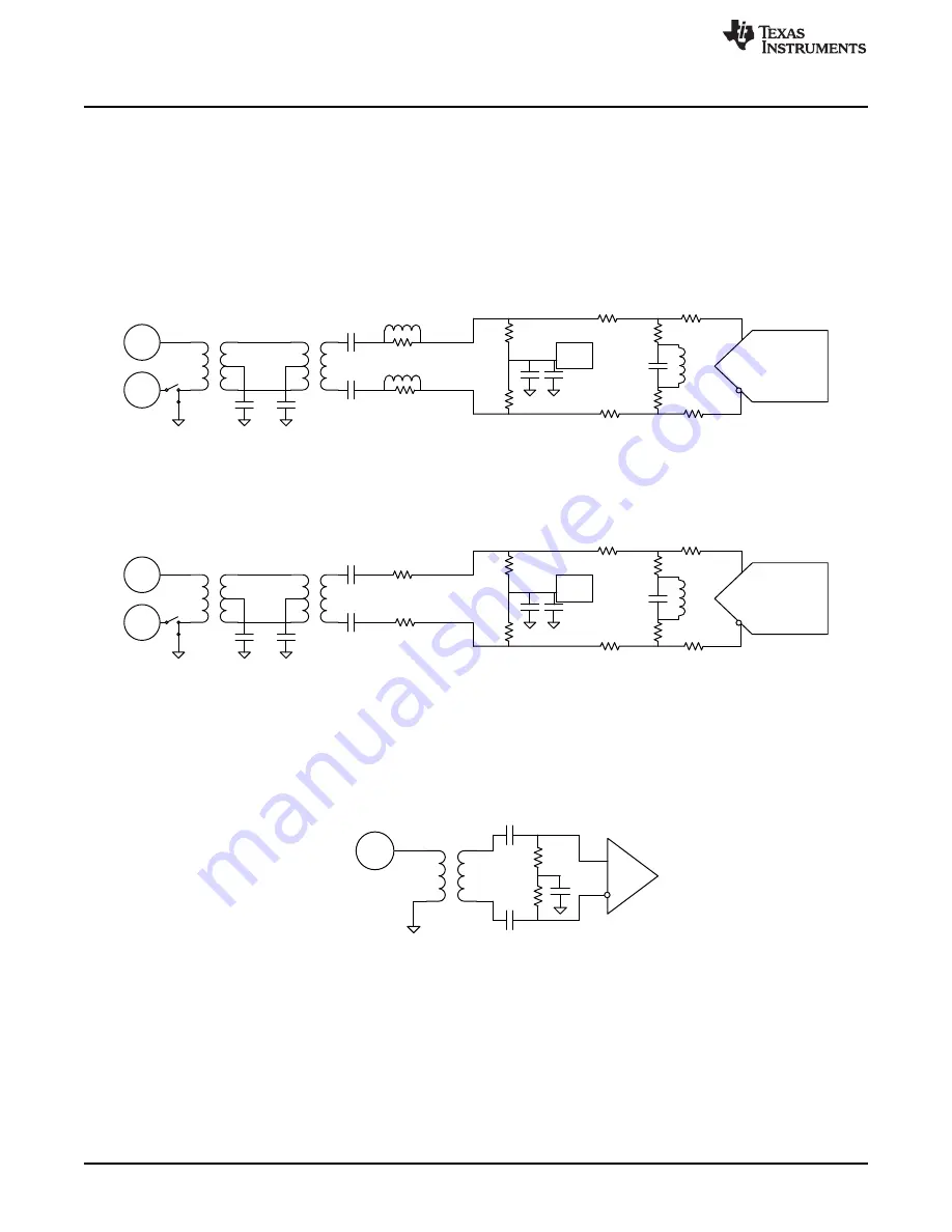
shows the ADC3xxxx ADC input circuit. The default setup has a dual 1:1 impedance ratio
transformer input circuit to achieve better phase and amplitude balance of the input signal than is typically
be produced by a single transformer input circuit.
The default input termination is 50
Ω
, which is formed by two 25-
Ω
resistors connected to the ADC VCM
node. By default, the input circuit is set for operation within the 1st two Nyquist zones. For higher
frequency inputs, use the high-frequency input circuit shown in
Figure 6. ADC3xxxx ADC Input Circuit Options
shows the ADC3xxxx clock input circuit. The clock signal goes through 1:4 impedance ratio
transformer to increase the clock amplitude by two (that is, 1:4 impedance ratio equals to 1:2 voltage
ratio). The two 100-
Ω
resistors impedance transform back to the primary side as 50-
Ω
load impedance for
the signal source generator. For ADC evaluation, set the signal generator output to approximately
+10 dBm.
Figure 7. ADC34xx Clock Input Circuit
1.5
EVM DC-Coupling Configuration
The ADC3xxxx EVM family has three different hardware configurations: dual-channel serial LVDS, quad-
channel serial LVDS, and quad-channel JESD204B compliant. The following instructions are a guideline to
enable dc-coupling on the revision B EVM hardware, but can be used as a guide for other EVM revisions.


