Software Control
16
SLAU579D – June 2014 – Revised August 2018
Copyright © 2014–2018, Texas Instruments Incorporated
ADC3xxxEVM and ADC3xJxxEVM
2.2.1.1
Common Register Tab
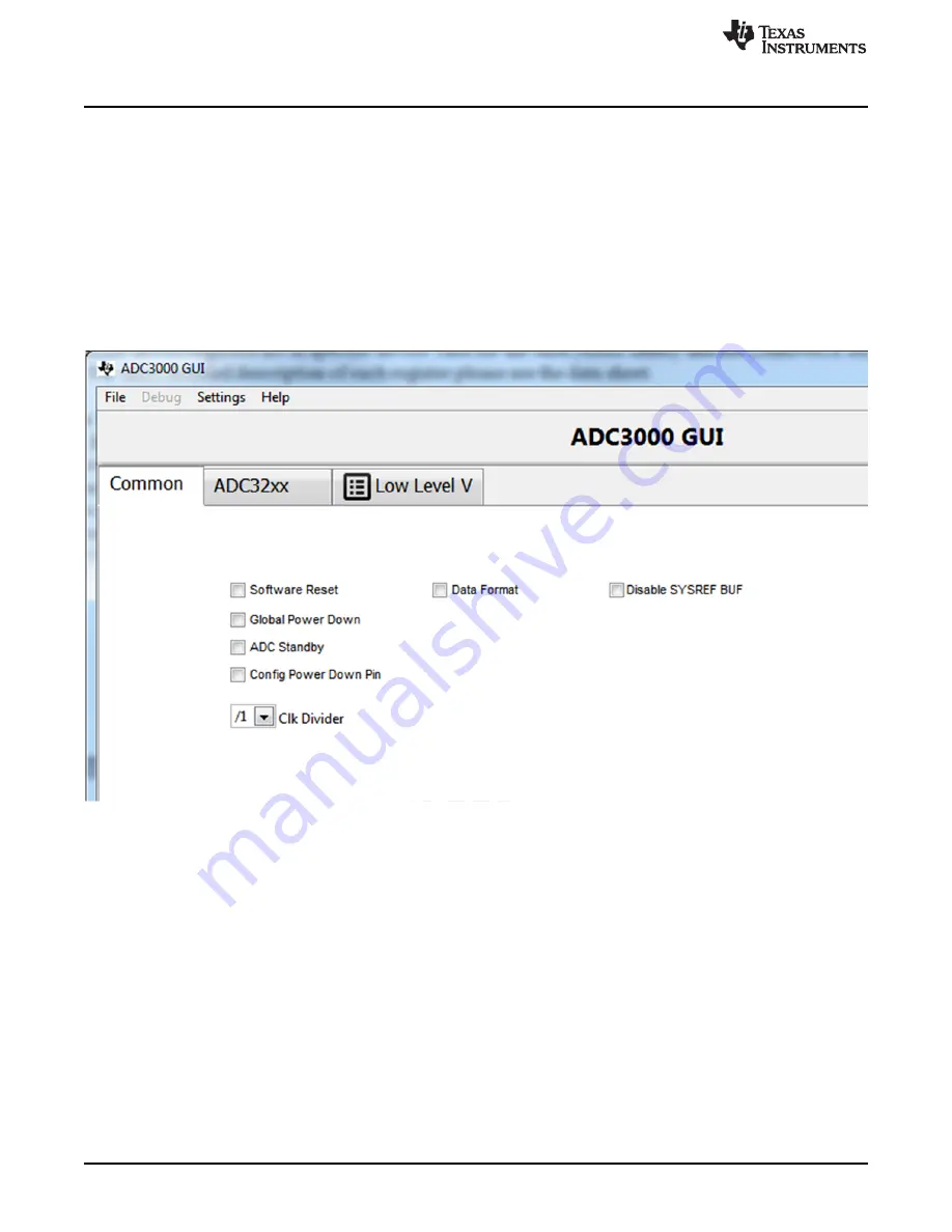
illustrates the following parts of the common tab.
•
Software Reset – Resets the registers to default configuration – similar to pressing SW1, self clearing
•
Global Power Down – power down the entire chip, default 0
•
ADC Standby – All ADCs enter standby mode, default 0
•
Configure PwDn pin function – either global power down or ADC standby mode
•
Data Format – 0 – 2s Complement, 1- Offset Binary, default 0
•
Disable SYSREF BUF – Disable SYSREF Buffer, default 0
•
Clk Diver – Internal clock divider to allow harmonic clocking, a higher frequency clock can be provided
to the ADC and then divided down to the desired sample rate.
Figure 10. Common Tab


