PC
USB
USB
J20
J17
USB Mini-B
Signal Generator
(Input Source)
LMK0
4828
CHB
J3
CHA
J1
+5V
J11
TSW14J56
J4
USB Mini-B
CHC
J5
CHD
J7
+5V
To A, B, C, D
Channels
BPF
Basic Test Procedure
27
SLAU579D – June 2014 – Revised August 2018
Copyright © 2014–2018, Texas Instruments Incorporated
ADC3xxxEVM and ADC3xJxxEVM
3.4
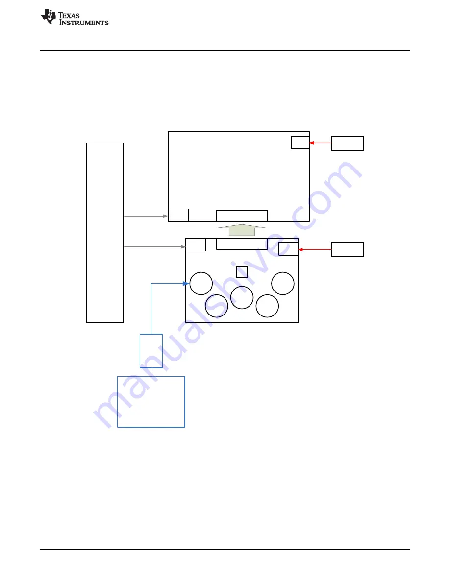
Test Block Diagram with ADC32Jxx and ADC34Jxx
The test set-up for evaluation of the ADC32J/34Jxx EVM with the TSW14J56 or TSW14J50 Capture Card
is shown in
. As seen in this figure, the evaluation setup involves a clock from a high quality on
board clock chip LMK04828 and a sine wave for the analog input from a high-quality signal generator.
High order, narrow bandpass filters are usually required to remove phase noise and harmonic content
from the input sine waves. Since the on board clock and input sinewave are not coherent then the
resulting FFT will need to have a windowing function such as Blackman-Harris/Hamming/Hanning applied
to the data.
Figure 18. ADC32Jxx/ADC34Jxx and TSW14J56 Test Setup Block Diagram


