background image

www.ti.com

Introduction

9

SLAU579D – June 2014 – Revised August 2018

Submit Documentation Feedback

Copyright © 2014–2018, Texas Instruments Incorporated

ADC3xxxEVM and ADC3xJxxEVM

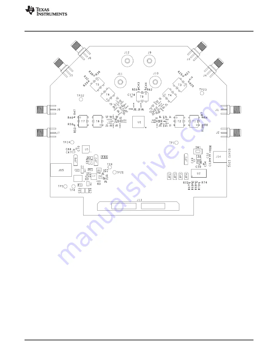
Figure 5. ADC34xx EVM Connector and Jumper Locations

The EVM has a barrel connector for 5-V power. The SMA connectors connect the ADC input and ADC
clock input to the ADC. Typically, the ADC inputs are transformer-coupled to accept single-ended
connections. The input circuit can be configured to connect to two SMA connectors for differential
signaling, if desired.

Table 3

lists the connector information for the ADC3xxxx.

Summary of Contents for ADC3221EVM

Page 1: ...uation module are synonymous with the ADC3xxx EVM and ADC3xJxx EVM unless otherwise noted Contents 1 Introduction 3 1 1 EVM Block Diagram 4 1 2 EVM Power Supply 6 1 3 EVM Connectors and Jumpers 8 1 4 EVM ADC Input Circuit Configurations 12 1 5 EVM DC Coupling Configuration 12 2 Software Control 15 2 1 Installation Instructions 15 2 2 Software Operation 15 3 Basic Test Procedure 24 3 1 Test Block D...

Page 2: ...x and TSW14J56 Test Setup Block Diagram 27 19 Select ADC32Jxx or 34Jxx in the HSDC Pro GUI Program 29 20 ADC32Jxx Operating in 14 Bit Mode at 160 MSPS With a 10 MHz Input Signal 30 List of Tables 1 ADC3xxx Family of Devices and EVMs 3 2 Power Supply Options 7 3 ADC3xxxx EVM Connectors 10 4 ADC3xxxx EVM Jumper Options 11 5 ADC3xxxx EVM LED Indicators 11 6 ADC32xxEVM AC DC Coupling Resistor Swap 13 ...

Page 3: ...3 12 80 ADC34J23EVM ADC34J24 12 125 ADC34J24EVM ADC34J25 12 160 ADC34J25EVM ADC34J42 14 50 ADC34J42EVM ADC34J43 14 80 ADC34J43EVM ADC34J44 14 125 ADC34J44EVM ADC34J45 14 160 ADC34J45EVM There are three package sizes and pinouts for all of these parts The sLVDS dual devices use a 7 mm 7 mm 48 pin QFN package The sLVDS quad devices use an 8 mm 8 mm 56 pin QFN package The dual and quad JESD204B devic...

Page 4: ...xEVM 1 1 EVM Block Diagram Figure 1 and Figure 2 show simplified block diagrams of the default configuration of the EVM The two or four analog inputs are supplied to the EVM through a single ended SMA connection then transformer coupled to turn the single ended signal into a balanced differential signal and then input to the ADC32xxx or ADC34xxx A dual transformer input circuit is used for better ...

Page 5: ...C3xJxxEVM Figure 2 Simplified ADC34J4x EVM Block Diagram The clock input is supplied by way of a single ended signal to an SMA connector and transformer coupled to produce a differential clock signal for the ADC32 34xx EVM For the ADC32J 34Jxx EVM the clock input can be generated onboard using the LMK04828 Power to the ADC3xxx EVM is typically supplied from a 5 V bench supply using the onboard bar...

Page 6: ... LMK04828 1 Low Noise LDO Introduction www ti com 6 SLAU579D June 2014 Revised August 2018 Submit Documentation Feedback Copyright 2014 2018 Texas Instruments Incorporated ADC3xxxEVM and ADC3xJxxEVM 1 2 EVM Power Supply Figure 3 illustrates the power supply options available on the ADC3xxx EVM Jumpers are used to choose the power supply options with the default jumper positions indicated by the da...

Page 7: ...U8 install R152 for 1 8 V switcher output JP12 1 2 JP13 1 2 Default connection for LDO 3 3 V for LMK04828 power and onboard SPI CPLD switch both to 2 3 to use U11 switcher output install R163 for 3 3 V switcher output The default power path has an efficient dual output DC DC switching power supply to first step down the input supplies from 5 V to 4 V and 2 8 V for the subsequent low noise LDOs The...

Page 8: ...umentation Feedback Copyright 2014 2018 Texas Instruments Incorporated ADC3xxxEVM and ADC3xJxxEVM 1 3 EVM Connectors and Jumpers Figure 4 and Figure 5 show the locations of the connectors jumpers pushbutton switches and LEDs Figure 4 ADC34Jxx EVM Connector and Jumper Locations ...

Page 9: ...Connector and Jumper Locations The EVM has a barrel connector for 5 V power The SMA connectors connect the ADC input and ADC clock input to the ADC Typically the ADC inputs are transformer coupled to accept single ended connections The input circuit can be configured to connect to two SMA connectors for differential signaling if desired Table 3 lists the connector information for the ADC3xxxx ...

Page 10: ...NI J11 SYSREF_INP positive input for SYSREF frame clock single ended input J12 SYSREF_INM negative SYSREF input DNI J13A B HSMC data connector to TSW1400 evaluation platform J14 Mini USB connector for SPI control J15 Power connector for 5 V adapter ADC32J 34Jxx J1 AIN_CH AP positive input for CHA single ended input DNI for ADC32Jxx J2 AIN_CH AM negative input DNI for ADC32Jxx and ADC34Jxx J3 BIN_C...

Page 11: ... JP6 2 pin default is connected for powering onboard VCXO SJP1 3 pin DNI optional for VCXO that require enable on pin 2 JP8 3 pin default 2 3 for USB SPI selection through CPLD 1 2 used for FMC connector based SPI port JP9 JP10 3 pin default 1 2 to use 1 8V LDO Use pins 2 3 to bypass LDO JP12 JP13 3 pin default 1 2 to use 3 3V LDO Use pins 2 3 to bypass LDO There is a pushbutton on the ADC3xxxx EV...

Page 12: ...d to the ADC VCM node By default the input circuit is set for operation within the 1st two Nyquist zones For higher frequency inputs use the high frequency input circuit shown in Figure 6 Figure 6 ADC3xxxx ADC Input Circuit Options Figure 7 shows the ADC3xxxx clock input circuit The clock signal goes through 1 4 impedance ratio transformer to increase the clock amplitude by two that is 1 4 impedan...

Page 13: ...tic design zip file This schematic details the components needed for dc coupling using the THS4541RGT and all required circuitry After the amplifier components are installed on the bottom of the ADC32xx EVM the resistors on the top of the board must be altered to change the output from ac coupled to dc coupled Figure 8 shows the three shared pad footprints per channel that must be modified See Tab...

Page 14: ...ors must be changed The output channels for dc coupled signals are B and C and the resistors are located near the baluns of the channel as shown in Figure 9 See Table 7 and the ADC34JxxEVM design files to change the appropriate resistors Table 7 ADC3xJxxEVM AC DC Coupling Resistor Swap Mode Install Uninstall AC Coupled R217 R258 R226R219 R233 R234 R137 R216 R225 R227R228 R218 R232 R235 DC Coupled ...

Page 15: ...ct Continue Downloading b Follow the on screen instructions to install the USB drivers c If needed access the drivers directly in the install directory 2 2 Software Operation The software allows programming control of the ADC3xxxx device The front panel provides a tab for full programming of the register map of the ADC3xxxx and an advanced tab that allows for custom register accesses The GUI tabs ...

Page 16: ...onfiguration similar to pressing SW1 self clearing Global Power Down power down the entire chip default 0 ADC Standby All ADCs enter standby mode default 0 Configure PwDn pin function either global power down or ADC standby mode Data Format 0 2s Complement 1 Offset Binary default 0 Disable SYSREF BUF Disable SYSREF Buffer default 0 Clk Diver Internal clock divider to allow harmonic clocking a high...

Page 17: ...gain setting from 0 dB to 6 dB Gain CHB digital gain setting from 0 dB to 6 dB Enable Test Pattern enable the use of test patterns instead of sample data Align Test Data align all test data on the outputs Test Pattern CHA different available test patterns Test Pattern CHB different available test patterns Custom Pattern 14 bit custom bit pattern used when Custom Pattern is selected Disable Chopper...

Page 18: ...tal gain setting from 0 dB to 6 dB Gain CHC digital gain setting from 0 dB to 6 dB Gain CHD digital gain setting from 0 dB to 6 dB Enable Test Pattern enable the use of test patterns instead of sample data Align Test Data align all test data on the outputs Test Pattern CHA different available test patterns Test Pattern CHB different available test patterns Test Pattern CHC different available test...

Page 19: ...www ti com Software Control 19 SLAU579D June 2014 Revised August 2018 Submit Documentation Feedback Copyright 2014 2018 Texas Instruments Incorporated ADC3xxxEVM and ADC3xJxxEVM Figure 12 ADC34xx Tab ...

Page 20: ...ed when Custom Pattern is selected SerDes Test Pattern available test patterns at the SerDes block Idle Sync Pattern pattern used for SYNC request K28 5 default Test Mode Enable option to enable long test pattern as per clause 5 1 6 3 Flip ADC Data normal operation is LSB first enable for MSB first Insert Lane Alignment Chars option to insert lane alignment chars as per clause 5 3 3 4 TX Link Conf...

Page 21: ...www ti com Software Control 21 SLAU579D June 2014 Revised August 2018 Submit Documentation Feedback Copyright 2014 2018 Texas Instruments Incorporated ADC3xxxEVM and ADC3xJxxEVM Figure 13 ADC32Jxx Tab ...

Page 22: ...utputs Test Pattern CHA different available test patterns Test Pattern CHB different available test patterns Test Pattern CHC different available test patterns Test Pattern CHD different available test patterns Custom Pattern 14 bit custom bit pattern to be used when Custom Pattern is selected SerDes Test Pattern available test patterns at the SerDes block Idle Sync Pattern pattern used for SYNC r...

Page 23: ...om ADS58H40 device not implemented in revision 1 x Save Regs Saves the register configuration for all devices Load Regs Load a register file for all devices Sample configuration files for common frequency plans are located in the install directory Select the Load Regs button Double click on the data folder Double click on the desired register file Click on Send All to ensure all the values are loa...

Page 24: ... Block Diagram with ADC32xx and ADC34xx Figure 15 shows the test set up for evaluation of the ADC3xxxx EVM with the TSW1400 Capture Card As seen in this figure the evaluation setup involves a clock from a high quality signal generator and a sine wave for the analog input from a high quality signal generator High order narrow bandpass filters are usually required on clock and input frequencies to r...

Page 25: ...t condition PDN is low JP2 JP3 JP4 JP5 Closed default condition for SPI connection JP6 1 2 default condition to select LDO power supply JP7 1 2 default condition to select LDO power supply 3 3 ADC32 34xx and TSW1400 Setup Guide See the TSW1400 user s guide for more detailed explanations of the TSW1400 set up and operation This document assumes the High Speed Data Converter HSDC Pro software and th...

Page 26: ...equency signal generator to the input frequency displayed The example shown in Figure 17 has the input frequency set at 10MHz 9 98878479MHx if coherent Filtered signal input around 10 dBm adjust to achieve 1 dBFs on the HSDC Pro FFT 7 Select channel 1 2 3 or 4 depending on the channel to which the signal generator is connected 8 Press the Capture button on the HSDC Pro GUI 9 Observe an FFT result ...

Page 27: ... 34Jxx EVM with the TSW14J56 or TSW14J50 Capture Card is shown in Figure 18 As seen in this figure the evaluation setup involves a clock from a high quality on board clock chip LMK04828 and a sine wave for the analog input from a high quality signal generator High order narrow bandpass filters are usually required to remove phase noise and harmonic content from the input sine waves Since the on bo...

Page 28: ...gramming The ADC32J 34Jxx EVMs require some programming for the on board clock requirements of the JESD204B interface 4 Provide a sine wave for the analog input at J3 or J6 of ADC32Jxx EVM and J1 J3 J5 or J7 of the ADC34Jxx EVM 5 Connect USB cable from the TSW14J56 to the programming computer 6 Verify the following jumper connections on the ADC32J 34Jxx EVM JP1 1 2 default condition PDN is low JP2...

Page 29: ...SPS_Operation_LMK_Setting cfg Check that the PLL2 LED D4 is lit this indicates that the PLL is programmed properly and the correct clocks are being generated 2 Start the HSDC Pro GUI program When the program starts select the ADC tab and then select ADC32Jxx_LMF_222 or ADC34Jxx_LMF_442 device in the Select ADC drop down menu Figure 19 Select ADC32Jxx or 34Jxx in the HSDC Pro GUI Program 3 When pro...

Page 30: ...orated ADC3xxxEVM and ADC3xJxxEVM Figure 20 ADC32Jxx Operating in 14 Bit Mode at 160 MSPS With a 10 MHz Input Signal If the basic capture at this point is correct then the front panel options of the ADC3xxx SPI GUI and the front panel options of the High Speed Data Converter Pro GUI may be varied as desired to test out different device SPI options ...

Page 31: ...on 24 Added reference to TSW14J50 in the Test Block Diagram with ADC32Jxx and ADC34Jxx section 27 Added reference to TSW14J50 in the Test Set up Connection Onboard LMK04828 Clock section 28 Changes from A Revision September 2014 to B Revision Page Changed the power supply reference to include options for using a 5 V brick or the provided power supply cable with barrel connector 5 Changes from Orig...

Page 32: ...y set forth above or credit User s account for such EVM TI s liability under this warranty shall be limited to EVMs that are returned during the warranty period to the address designated by TI and that are determined by TI not to conform to such warranty If TI elects to repair or replace such EVM TI shall have a reasonable time to repair such EVM or provide replacements Repaired EVMs shall be warr...

Page 33: ...the user guide with the maximum permissible gain and required antenna impedance for each antenna type indicated Antenna types not included in this list having a gain greater than the maximum gain indicated for that type are strictly prohibited for use with this device Concernant les EVMs avec antennes détachables Conformément à la réglementation d Industrie Canada le présent émetteur radio peut fo...

Page 34: ...ed loads Any loads applied outside of the specified output range may also result in unintended and or inaccurate operation and or possible permanent damage to the EVM and or interface electronics Please consult the EVM user guide prior to connecting any load to the EVM output If there is uncertainty as to the load specification please contact a TI field representative During normal operation even ...

Page 35: ...COST OF REMOVAL OR REINSTALLATION ANCILLARY COSTS TO THE PROCUREMENT OF SUBSTITUTE GOODS OR SERVICES RETESTING OUTSIDE COMPUTER TIME LABOR COSTS LOSS OF GOODWILL LOSS OF PROFITS LOSS OF SAVINGS LOSS OF USE LOSS OF DATA OR BUSINESS INTERRUPTION NO CLAIM SUIT OR ACTION SHALL BE BROUGHT AGAINST TI MORE THAN TWELVE 12 MONTHS AFTER THE EVENT THAT GAVE RISE TO THE CAUSE OF ACTION HAS OCCURRED 8 2 Specif...

Page 36: ... TI Resource NO OTHER LICENSE EXPRESS OR IMPLIED BY ESTOPPEL OR OTHERWISE TO ANY OTHER TI INTELLECTUAL PROPERTY RIGHT AND NO LICENSE TO ANY TECHNOLOGY OR INTELLECTUAL PROPERTY RIGHT OF TI OR ANY THIRD PARTY IS GRANTED HEREIN including but not limited to any patent right copyright mask work right or other intellectual property right relating to any combination machine or process in which TI product...

Reviews: