5 Onboard Clocking Hardware Setup
The onboard CDC is useful for general evaluation and relieves the user requirment of needing additional signal
generators. However, the clock spurs and jitter of the CDCE6214 (due to 4.5 sample clock/DCLKIN relationship)
begin to effect the optimal ADC AC performance.
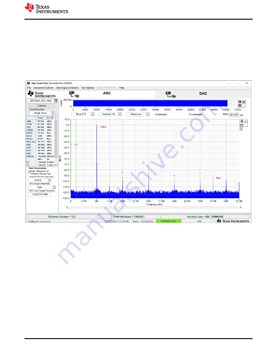
Looking at the image below, we can see that SNR/SFDR performance does degrade by several dBFS for the
ADC3663EVM, however, using the onboard CDCE6214 relieves the user of providing the external sample clock
and DCLKIN, and may be useful for verifying the SLVDS interface to an FPGA development kit. In practice, an
appropriate filter may be used to reduce the effects of clock spurs and broad band phase noise in order to
acheive full ADC performance.
Figure 5-1. ADC3663EVM onboard clocking (CDCE6214: 65 MHz sample clock, 260 MHz DCLKIN)
The following section shows how to configure and program the ADC366xEVM for onboard clock operation for
Real Decimation Mode. Onboard clocking can be used for Bypass and Complex Decimation modes as well, and
uses similar procedures that have been outlined in this document.
When using onboard clocking, there are several different sampling rates to choose from (65MSPS, 25 MSPS
and 10 MSPS) in Bypass and Decimation modes. The ADC35XX GUI does not support configuring the
CDCE6214 to frequencies outside of these preset selections at this time.
Onboard Clocking Hardware Setup
SBAU366 – JANUARY 2021
ADC366xEVM Evaluation Module
19
Copyright © 2021 Texas Instruments Incorporated


