Printed Circuit Board Layout
4-3
Schematic and Layout
4.2
Printed Circuit Board Layout
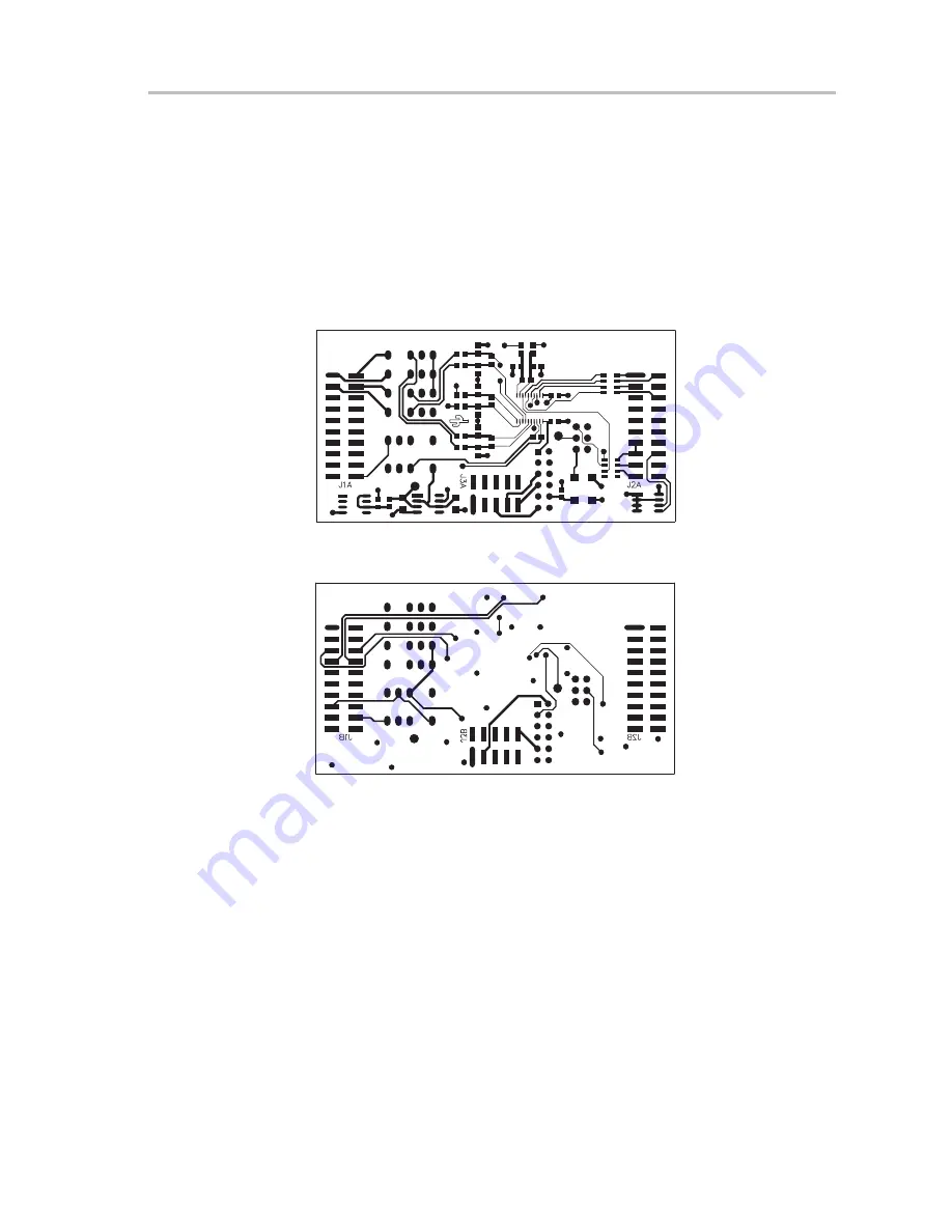
The ADS1224EVM is a four-layer PCB. The layer stack order, from top to
bottom, is component (top) layer, ground plane, power plane, and solder
(bottom) layer.
Four layers were necessary to accommodate the many components on the
board. Four layers are not necessary for high performance with the ADS1224;
the same level of performance can also be achieved on a two-layer board.
Figure 4−2. Top Side Layout
Figure 4−3. Bottom Side Layout
Summary of Contents for ADS1224EVM
Page 1: ... April 2004 User s Guide SBAU095 Data Acquisition Products ...
Page 14: ...Setting Up 1 6 ...
Page 30: ...Clock Circuitry 3 4 ...


